
Datasheet


NCP3066, NCV3066
http://onsemi.com
2
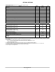
Figure 2. Pin Connections
Timing Capacitor
Comparator
Inverting
Input
V
CC
ON/OFF
I
pk
Sense
GND
Switch Emitter
Switch Collector
(Top View)
4
3
2
1
5
6
7
8
Comparator
Inverting
Input
V
CC
ON/OFF
I
pk
Sense
Timing Capacitor
GND
Switch Emitter
Switch Collector
(Top View)
Figure 3. Pin Connections
NOTE: EP Flag must be tied to GND Pin 4 on PCB
EP Flag
SOIC−8/PDIP−8 DFN8
Figure 4. Block Diagram
5
R
S
Q
+
−
7
Comparator
CT
3
8
TSD
0.2 V
+
−
2
6
R
S
Q
4
1
Switch Collector
Switch Emitter
Timing Capacitor
GND
Comparator Inverting Input
V
CC
I
pk
Sense
ON/OFF
Oscillator
0.235V
Reference
Regulator
ON/OFF
Bias
Comparator
PIN DESCRIPTION
Pin No.
Pin Name Description
PDIP8 DFN8
1 1 Switch Collector Internal Darlington switch collector.
2 2 Switch Emitter Internal Darlington switch emitter.
3 3 Timing Capacitor Timing Capacitor to control the switching frequency.
4 4, EP Flag GND Ground pin for all internal circuits.
5 5 Comparator Inverting Input Inverting input pin of internal comparator.
6 6 V
CC
Voltage Supply
7 7 I
pk
Sense Peak Current Sense Input to monitor the voltage drop across an external
resistor to limit the peak current through the circuit.
8 8 ON/OFF ON/OFF Pin. To disable the device, this input should be pulled below
0.8 V. If the pin is left floating, it will be disabled.