
Datasheet


NCP3066, NCV3066
http://onsemi.com
8
Peak Current Sense Comparator
Under normal conditions, the output switch conduction is
initiated by the Voltage Feedback comparator and
terminated by the oscillator. Abnormal operating conditions
occur when the converter output is overloaded or when
feedback voltage sensing is lost. Under these conditions, the
I
pk
Current Sense comparator will protect the Darlington
output Switch. The switch current is converted to a voltage
by inserting a fractional ohm resistor, R
Sense
, in series with
V
CC
and Darlington output switch. The voltage drop across
R
Sense
is monitored by the Current Sense comparator. If the
voltage drop exceeds 200 mV (nom) with respect to V
CC
, the
comparator will set the latch and terminate the output switch
conduction on a cycle−by−cycle basis.
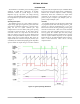
Real
V
turn−off
on
R
s
Resistor
t_delay
I1
Io
di/dt slope
I through the
Darlington
Switch
V
ipk(sense)
Figure 13. Current Sense Waveform
The V
IPK(Sense)
Current Limit Sense Voltage threshold is
specified at static conditions. In dynamic operation the
sensed current turn−off value depends on comparator
response time and di/dt current slope.
Real V
turn−off
on R
sc
resistor
V
turn_off
= V
ipk(sense)
+ R
Sense
*(t
delay
*di/dt)
Typical I
pk
comparator response time t
delay
is 350 ns. The
di/dt current slope is dependent on the voltage difference
across the inductor and the value of the inductor. Increasing
the value of the inductor will reduce the di/dt slope.
It is recommended to verify the actual peak current in the
application at worst conditions to be sure that the max peak
current will never get over the 1.5 A Darlington Switch
Current max rating.
Thermal Shutdown
Internal thermal shutdown circuitry is provided to protect
the IC in the event that the maximum junction temperature
is exceeded. When activated, typically at 160°C, the
Darlington Output Switch is disabled. The temperature
sensing circuit is designed with some hysteresis. The
Darlington Switch is enabled again when the chip
temperature decreases under the low threshold. This feature
is provided to prevent catastrophic failures from accidental
device overheating. It is not intended to be used as a
replacement for proper heatsinking.
Output Switch
The output switch is designed in Darlington
configuration. This allows the application designer to
operate at all conditions at high switching speed and low
voltage drop. The Darlington Output Switch is designed to
switch a maximum of 40 V collector to emitter voltage and
current up to 1.5 A.
ON/OFF Function
The ON/OFF function provides interruption of switching
and puts the circuitry into the low consumption mode. This
feature is applicable for digital dimming of the LEDs as
well. The ON/OFF signal inhibits switching of the regulator
and reduces the average current through the LEDs. The
frequency of this pulse width−modulated signal with the
duty cycle can range from less than 1% to 100% is limited
by the value of 1 kHz.
Pulling this pin below 0.8 V or leaving it opened turns the
regulator off. In this state the consumption of the device is
reduced below 100 uA. Pulling this pin above 2.4 V (up to
max. 25 V) allows the regulator running in normal state. If
the ON/OFF feature is not needed, the ON/OFF pin can be
wired to V
CC
, provided this voltage does not exceed 25 V.
No Output Capacitor Operation
A traditional buck topology includes an inductor followed
by an output capacitor which filters the ripple. The capacitor
is placed in parallel with the LED or array of LEDs to lower
the ripple current. A constant current buck regulator such as
the NCP3066 focuses on the control of the current through
the load, not the voltage across it. The switching frequency
of the NCP3066 is in the range of 100−250 kHz which is
much higher than the human eye can detect. By configuring
the NCP3066 in a continuous conduction buck
configuration with low peak to peak ripple the output filter
capacitor can be eliminated. The important design
parameter is to keep the peak current below the maximum
current rating of the LED. Using 15−40% peak to peak ripple
results in a good compromise between achieving max
average output current without exceeding the maximum
limit. This saves space and reduces part count for
applications.