www.osram.com/oled Application guide.
CONTENTS 2
CONTENTS 1. OLED integration 1.1. General handling instructions 1.2. Contact ledges and their polarity 1.3. Interconnection 1.4. Contacting of OLED tiles via conductive glue 1.5. Contacting of OLED tiles via elastomeric connectors 1.6. Contacting via Flex-PCB 4 4 5 6 6 7 8 2. Binning 2.1. Color binning 2.2. Luminance binning 10 10 12 3. Driving 13 4. Reliability 4.1. Maximum ratings 4.2. Degradation 4.2.1. Absolute value of initial luminance 4.2.2. Ambient temperature 4.3. Lifetime 4.4. Robustness 4.
OLED INTEGRATION 1. OLED integration 1.1. General handling instructions Remember when handling OLED devices: First and foremost, OLEDs are made of glass and glass is fragile. 4 • Avoid mechanical stress such as shock and pressure on the glass during handling, especially at the center of the active area and the back of the device (to avoid glass cracking, delamination and damage of the internal structure).
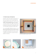
OLED INTEGRATION 1.2. Contact ledges and their polarity OLED devices without Flex-PCB (for Flex-PCB, please see below) are electrically connected via the metallized areas at the contact ledges (see fig. 1). Usually, symbols at the metallization indicate the polarity of the contacts. For round ORBEOS® (CDW-031, CMW-031) devices, the cathode contacts can be identified when looking at the emissive side of the device: Cathode contacts exhibit a comb structure at the edge of the active area (see fig. 2).
OLED INTEGRATION 1.3. Interconnection On the following pages, several techniques for interconnecting OLEDs are described. To interconnect OLED devices, their contact surfaces have to be free of dust and grease. If necessary, use isopropyl alcohol (IPA) to carefully wipe the contact ledges clean. In general, the interconnection should be applied without heat introduction into the active area of the device. Furthermore, avoid mechanical stress.
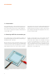
OLED INTEGRATION 1.5. Contacting of OLED tiles via elastomeric connectors In this example, elastomeric connectors are used for interconnecting OLEDs. Similar low-resistance connectors can be used accordingly. The product can be acquired from Nucletron Technologies GmbH, Munich. The connectors should cover the contact ledges completely to minimize contact resistance. They have to be compressed by 5 – 25 % of their height to ensure optimal conductivity and vibration resistance.
OLED INTEGRATION a b c Fig. 5. Free-standing Flex-PCB with four flaps (a) attached to an ORBEOS® CMW-031 (b). The eight golden soldering pads of the Flex-PCB are visible. Each one provides a positive and negative pole as well as a through contact “0”. ORBEOS® RMW-046 (c) can be equipped with a flex connector with two soldering pads on both sides (front side and back side). 1.6.
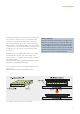
OLED INTEGRATION Flex-PCBs are applied by a special conductive polymer material in a thermo-compression process called ACF bonding (anisotropic conductive film bonding), which is well known from the display industry: First, a two-component material is dispensed at the contact pad of the OLED. Then, the Flex-PCB is adjusted to the contact pad. Afterwards, heat and pressure is applied on the connection by a heated stamp (bonding tool, figure 7).
BINNING 2. Binning Solid-state lighting products are usually classified into color and brightness bins in order to meet customer demands and deliver as narrow selections as possible. For ORBEOS® products, the binning schemes are explained in the following sections. 2.1. Color binning A widely-used standard for the classification of chromaticity in SSL application is “ANSI_NEMA_ANSLG C78.377-2008” (http://www.nema.org/stds/ANSI-ANSLG-C78-377.cfm).
BINNING OSRAM has established a finer resolution classification and has divided the ANSI-NEMA color boxes into smaller sub-bins (so called “fine-bins”). In order to cover the full production output, a row of sub-bins of similar size have been introduced above and below the ANSI-NEMA boxes. The scheme is shown in figure 9. In this binning scheme, the size of one fine-bin box roughly corresponds to a three-step MacAdam ellipse.
BINNING 2.2. Luminance binning Brightness binning of OLEDs is slightly different than for LED products. While inorganic LEDs rely on luminous intensity or luminous flux binning, the most reasonable quantity for OLED products is the luminance. For ORBEOS® products, the binning scheme is characterized by a double-digit system. The first digit denotes the rough luminance class.
DRIVING/RELIABILITY 3. Driving In general, OLEDs are driven in constant current mode. If dimming is required, it is recommended to use PWM (pulse width modulation). Besides, it is also possible to adjust the driving current. Please note that current modulation may influence the color coordinates of the emitted light. If a constant-current source design for LEDs is used, make sure that the power supply doesn’t generate current and/or voltage overshoots while switching it on or off.
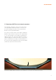
Relative luminance [L/L0] RELIABILITY 1.00 Initial luminance = 50 % of standard Standard initial luminance 0.75 0.50 0.25 0 0 2,500 5,000 7,500 10,000 12,500 15,000 17,500 Operating time [h] Fig. 10. Luminance degradation characteristics of an OLED with two different initial luminance values (normalized luminance values). The lower curve shows a drop to 50 % of the initial value after approximately 5,000 hours.
RELIABILITY 4.4. Robustness In the following paragraphs, some indications are given on the ruggedness of OLEDs and their stability against some environmental conditions. 4.4.1. Mechanical pressure, shock and vibration OLEDs are made of glass, meaning that mechanical forces may cause glass breaks. One special case is local pressure on the back side of a cavity-glass-encapsulated OLED.
APPENDIX Appendix Corner values (CIE coordinates) of all 4C9X fine-bins Bin cx cy Bin cx cy Bin cx cy Bin cx cy 8C 0.3028 0.3304 8J 0.3548 0.3736 9Q 0.4198 0.4115 9W 0.4688 0.429 0.3015 0.3368 0.356 0.3826 0.4232 0.4201 0.4739 0.4382 0.3076 0.343 0.3659 0.3899 0.4337 0.4253 0.4803 0.4398 0.3087 0.3363 0.3642 0.3805 0.4299 0.4165 0.475 0.4304 0.3041 0.324 0.3536 0.3646 0.4164 0.4029 0.4636 0.4197 0.3028 0.3304 0.3548 0.3736 0.4198 0.4115 0.
APPENDIX Corner values (CIE coordinates) of all 4C9X fine-bins Bin cx cy Bin cx cy Bin cx cy Bin cx cy 7E 0.3154 0.3352 7L 0.3714 0.3775 4R 0.4109 0.3726 4X 0.4485 0.3838 0.3146 0.3422 0.3736 0.3874 0.4147 0.3814 0.4538 0.3931 0.3205 0.3481 0.3826 0.3931 0.4222 0.384 0.4593 0.3944 0.321 0.3408 0.3799 0.3828 0.4181 0.3751 0.4538 0.385 0.3162 0.3282 0.3692 0.3677 0.4387 0.4197 0.3154 0.3352 0.3714 0.3775 0.4428 0.4286 0.321 0.3408 0.3799 0.
APPENDIX Corner values (CIE coordinates) of all 4C9X fine-bins Bin 6G 5G 4G 8H 7H 6H 5H 4H 8I 7I 6I 18 cx cy Bin cx cy Bin cx cy 6N 5T 0.3293 0.3384 0.3853 0.3776 0.4298 0.3867 0.3292 0.3461 0.3885 0.3882 0.4342 0.3957 0.3373 0.3534 0.397 0.3935 0.442 0.3985 0.3369 0.3451 0.3934 0.3825 0.4373 0.3893 0.3294 0.3306 0.3822 0.367 0.4253 0.3776 0.3293 0.3384 0.3853 0.3776 0.4298 0.3867 0.3369 0.3451 0.3934 0.3825 0.4373 0.3893 0.3366 0.3369 0.
APPENDIX Corner values (CIE coordinates) of all 4C9X fine-bins Bin 5I 4I cx cy Bin cx cy Bin cx cy 7P 6V 0.344 0.3428 0.4036 0.3898 0.4477 0.3998 0.3448 0.3515 0.4067 0.3982 0.4526 0.409 0.3527 0.3578 0.4164 0.4029 0.4585 0.4104 0.3515 0.3487 0.4129 0.3944 0.4534 0.4011 0.3433 0.3341 0.4006 0.3815 0.4428 0.3906 0.344 0.3428 0.4036 0.3898 0.4477 0.3998 0.3515 0.3487 0.4129 0.3944 0.4534 0.4011 0.3503 0.3396 0.4095 0.3858 0.4483 0.3918 0.3975 0.
www.osram.com/oled Global presence. OSRAM supplies customers in 148 countries. • 85 companies and sales offices for 122 countries • 26 countries served by local agents or OSRAM GmbH, Munich OSRAM associated companies and support centers: OSRAM GmbH Head Office Hellabrunner Strasse 1 81543 Munich Phone +49 (0) 89-6213-0 Fax +49 (0) 89-6213-20 20 www.osram.