
User Manual


A432 Radio Module UM.docx Page 3 of 5
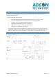
THE MODULE CONNECTOR
All control signals and supply voltages are accessible via the 24 pin connector P2.
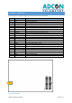
PIN Name Function
1 VPA PA power supply, 3.6 V
2 VPA PA power supply, 3.6 V
3 VDD_IN Power supply, 3.0 V
4 RFMOD_ON RF module enable, HIGH = enable
5 SCLK SPI clock
6 SO SPI serial data output
7 SI SPI serial data input
8 -CSRF SPI chip select, LOW = selected
9 -CCRESET Reset signal for transceiver chip, LOW = reset
10 RXDATA Received data output
11 TXDATA Transmit data input
12 RXTXCLK Receive/transmit clock
13 RXEN Receiver enable
14 TXEN Transmitter enable
15 POUT Output power measurement
16 -FEEN Front end enable, LOW = enable
17 VCTCXO_ON VCTCXO enable input, HIGH = enable
18 LBS Low band select, 430 – 450 MHz
19 HBS High band select, 450 – 470 MHz
20 -CSFTUNE Chip select frequency fine tune
21 CFG0 HW configuration bit 0
22 CFG1 HW configuration bit 1
23 CFG2 HW configuration bit 2
24 GND Ground connection
3 additional GND connections are made by the module mounting holes.
Figure 1, Module Bottom Side
P1