Panasonic Service and Technology Company Technical Guide 10th Generation Plasma Display Television National Training
Panasonic Service and Technology Company Prepared by Cesar Perdomo and Jean Magloire Panasonic Service and Technology Company National Training Copyright © 2007 by Panasonic Services Company All rights reserved. Unauthorized copying and distribution is a violation of law. Warning This service information is designed for experienced repair technicians only and is not designed for use by the general public.
Table of Contents Subject Page # Subject Page # 2007 Panasonic Plasma Line-up 5 Troubleshooting (No Power/Dead Unit) Part 2 56 Models Comparison 6 SOS Circuit Overview 59 High Resolution (FULL-HD Panel) 9 DRV_RST SOS 62 TH-42PX75U Board Layout & Description 13 Location of Q9302 63 TH-42PX75U Board Layout (Pictorial) 14 Close-up View of Q9302 64 2006/2007 Signal Process/Switching Circuit 15 5 Blinks SOS (1) 66 Overall Block Diagram 16 SOS (Drive-reset) 68 Standby Circuit 21
Table of Contents (Continued) Subject Page # Driver Setup Adjustment 96 Initialization Pulse Adjustment 97 Quick adjustment after P.C.B.
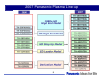
2007 Panasonic Plasma Line-up 5
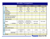
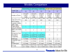
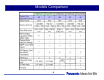
Models Comparison 6
Models Comparison 7
Models Comparison 8
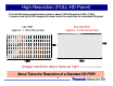
High Resolution (FULL-HD Panel) The Full-HD plasma panel boasts a total of about 2,070,000 pixels (1920 x 1080). It renders true-to-life HD images with about twice the resolution of a standard HD panel. Full-HD PDP (approx. 2,070,000 pixels) HD PDP (approx.
10th Generation Plasma Television Board Layout 11
TH-42PX75U Boards Layout & Description Panasonic started using single scan addressing in the 42” HD models last year when the 9th generation of Plasma TV was introduced. The single scan addressing was only used on standard definition models previously. For this generation, Panasonic has added the 50” models to the list of TV using single scan addressing.
TH-42PX75U Board Layout (Pictorial) 14
2006/2007 Signal Process/Switching Circuit The 2007 42” plasma models have less boards than the previous generation. The PA, DT, DG, H, and HC boards used on the 2006 42” models are now incorporated within the new A board of the 2007 models.
Overall Block Diagram 16
Overall Block Diagram The operation of the plasma TV can be divided into 3 different sections: 1. Power Supply Circuit The power supply circuit board (P board) provides voltages to the Signal switching/processing circuit and the Panel drive circuit. 2. Signal Switching/Processing Circuit Upon connecting the unit to the AC voltage source, the STB5V of the P board is provided to the A board for system control operation.
10th Generation Plasma Television Power Supply 19
Standby Circuit 21
Standby Circuit 1. When the TV is connected to the AC line, the power supply outputs 5V. 2. This voltage is applied to the D board and the A board. The 5V applied to the D board in the Panel Drive Section is not used during standby operation. 3. On the other hand, when the A board receives the 5V from the Power supply, it outputs the “F_STB_ON” command. 4. This command is applied to the power supply board to generate the F_STB15V.
Standby Circuit 23
Standby Circuit When AC is applied to the TV, the Standby circuit outputs 5Vdc and 12Vdc. The 5V is applied to the Power MCU and the switching transistor Q537 of the power supply circuit. The 12V is provided to the SS board. A jumper at connector SS34 of the SS board routes the 12V back into the power supply board to turn on Q537. When Q537 is on, the STB5V is output to the D and A boards. On the D board, the STB5V is applied to a 3.3V regulator (IC9011).
STB5V/STB3.3V Distribution The STB5V is connected to the D and A boards. During standby, this voltage is not used by the D board. On the A board, the STB5V is applied to a 3.3V regulator (IC5604) to generate the STB3.3V to power the MAIN MICON Genx4 (IC1100). The STB3.3V is also connected to the remote receiver IC and the power LED on the K board.
STB5V (2) P25 This circuit combined with the circuit in the following page is used to explain the reason why the CPU (IC9003) on the D board is not active during Standby. The transistor Q9014 is on to keep PANEL_STBY_ON low.
STB5V (3) The STB5V source is connected to the voltage input (pin 4) of the RESET/STB3.3V regulator IC9011. The output of this IC is controlled by the ON/OFF pin (Pin 6). The DC level of this pin is determined by the “STB3.3V ON/OFF” circuit. During standby pin 6 of IC9011 is low keeping IC9011 off. When the power is turned on; pin 6 goes high, the IC turns on and outputs 3.3V on pin 3.
Main CPU VCC Supply (A Board) 28
Main CPU VCC Supply (A Board) On the A board, the STB5V is applied to pins 3 and 4 of the 3.3V regulator (IC5604). Pin 4 is the voltage input to the IC and pin 3 is the ON/OFF command. The STB5V at pin 3 allows pin 5 to output 3.3V. The 3.3V from IC5604 is then applied to pins 31, 50, 74, 78, 81, 85, and 100 of the CPU (IC1100). This turns on the main CPU (IC1100) and a high command (TV_SUB_ON/TUNER_SUB_ON) is output on pin 1. This command splits in 2 (TUNER_SUB_ON and TV_SUB_ON).
TV_SUB_ON/TUNER_SUB_ON 30
TV_SUB_ON/TUNER_SUB_ON The STB 5V at pin 5 of connector A7 and the TV SUB ON command at pin 6 are used to activate the PA SOS detect circuit on the A board. This circuit monitors the F+15V, DT9V, and SUB5V for abnormality. Under normal operation, the TUNER_SUB_ON voltage from pin 1 of the main CPU (IC1101) turns on Q3504. When Q3504 is on, a low is applied to the base of Q3502 turning it on. When Q3502 is on, 5V is applied to the emitter and base of Q3503.
TV_SUB_ON (F_STB_ON) P Board P 32
TV_SUB_ON (F_STB_ON) The F-STB-ON voltage (3.2V) from pin 6 of connector P7 is applied to pin 23 of the Power CPU (IC501) on the P board. IC501 sends out commands to first turn on the primary circuit of the power supply, and then the circuit that allows the F_STB15V to develop. 1. 2. The relay commands (high) from pins 11 and 12 of IC501 are used to trigger the relays RL402 and RL403. A low from pin 16 of IC501 is used to turn on the power factor control IC (IC406) to generate the 395V DC. 3.
TV_SUB_ON (Relay Drive Circuit) 34
TV_SUB_ON (Relay Drive Circuit) The F_STBY_ON voltage (3.2V) from pin 6 of connector P7 is applied to pin 23 of the power MCU (IC501) on the P board. When pin 23 goes “high”, pin 12 goes “high” turning on Q502 to trigger the inrush relay RL403. Approximately 300ms later, pin 11 also goes ”high” turning on Q501 to trigger the main relay RL402. 300ms later, pin 12 goes “low” allowing for only the main relay RL402 to remain on. RL401 is triggered whenever RL402 or RL403 are triggered.
PFC Circuit Pin 16 of IC501 also goes low when pin 23 is “high”. When pin 16 goes “low”, the diode within the photo-coupler IC401 emits light to turn on the photo-transistor. Pin 4 of IC401 goes “low”. This “low” is applied to the gate of Q401 turning it on to apply 12V to pin 8 of PFC circuit.
ACFB (Active Clamp Full Bridge Switching) Circuit 37
ACFB (Active Clamp Full Bridge Switching) Circuit The PFC 395VDC is applied to the switching circuit (Q408, Q409, Q412, and Q413). The operation of this switching circuit is controlled by the transformer T402 which is driven by the V-low power control IC, IC520. 1. A “high” from pin 15 of IC501 is used to turn on the power control IC (IC520) to energize the primary of transformer T402 and allow the switching circuit to drive transformer T404. 2.
MAIN/SUB Voltages 39
MAIN/SUB Voltages The F+15V from the power supply is applied to pins 6, 7, and 8 of connector A6 on the A board. The 15V is applied to the voltage input pin (pin 9) of the “SUB+5V/SUB+9V” dual regulator IC3500. The 15V is also used to keep pin 1 and pin 15 high. Pin 1 and pin 15 are the “ON/OFF” pins. When pin 1 is high, pin 3 outputs 5V. When pin 15 is high, pin 13 outputs 9V. D3500 monitors the 15V line for “OVER VOLTAGE” condition. If the 15V becomes excessive, D3500 conducts to turn on Q3500.
F+15V, DTV9V, SUB5V SOS Detect Circuit 41
F+15V, DTV9V, SUB5V SOS Detect Circuit The F+15V, DTV9V, and SUB5V are monitored for over-voltage and over-current conditions by the SOS circuit on the A board. Under normal condition, pin 114 of the main CPU (IC1100) is low. When a short circuit or an over-voltage condition occurs, the SOS detect circuit is triggered causing pin 114 to go high. When pin 114 goes high, the TV shuts down and the power LED blinks 10 times. When the F+STB15V line is shorted, the base of Q3503 goes low turning it on.
Power On Operation 43
Power On Operation The power command from the power switch on the S board or the remote control receiver on the K board is provided to the CPU in the A board. The CPU on the A board outputs the “PANEL_STB_ON” command and the “F_STB_ON” command. The “PANEL_STB_ON” is provided to the D board to turn on the STB3.3V regulator. The output voltage is applied to the CPU in the D board. The “F_STB_ON” command is provided to the power supply to develop the F_STB+15V.
Power-On (1) L 45 H
Power-On (1) When the unit is turned on using the power button on the front of the TV, the momentary connection of the power switch to ground supplies a low to the base of Q5604 (DG board) to turn it on. Q5604 outputs a low to the key input line (pin 18) of the CPU IC1100 on the A board. The R/C receiver receives the power on command of the remote control and outputs the IR data to the amplifier Q2510 of the A board. The data is amplified and output to pin 45 of the MPU, IC1100.
Power On (2) Upon receiving the power on command , the “PANEL STB/VCC ON” pin of the main MPU (IC1100) outputs 2.5V to the base of Q4015, turning it on. Q4015 outputs a low to turn off Q4014 allowing pin 20 of the connector A5/D5 to go high.
Power On (3) 48
Power On (3) The STBY5V from the power supply board is applied to pin 4 of the regulator, IC9011. During Standby operation, the regulator does not operate due pin 6 being low. Upon receiving the power on command , the “PANEL STB ON” high from pin 20 of connector D5 is applied to the base of Q9044 on the D board, turning it on. Q9044 outputs a low to turn off Q9046. When pin 6 goes high, IC9011 outputs the reset command at pin 1 and the STB3.3V at pin 3. The STB3.
Power On (Summary) When the power is turned on, the “PANEL MAIN ON” command and the “F STB ON” command are applied to the power MCU (IC501). The complete standby operation is repeated when the “F STB ON” command from the A board is applied to pin 23. When the (3.2V) “PANEL MAIN ON” command from the D board is applied to pin 24 of IC501, pin 10 goes high and pin 14 goes low. The high from pin 10 turns on the 15V DC-DC converter (Q555) to output the P15V.
P15V/P5V Circuit 51
P15V/P5V Circuit The P15V is generated when the power is turned on. The high (3.2V) “Panel Main On” command from the D board is applied to pin 24 of the Power MCU (IC501) on the Power Supply board. When IC501 receives this command on pin 24 (3.2V), pin 10 goes high (4.8V). When the power on command is received, the F_STB_ON command (3.2V) is applied to pin 23 of IC501.
Vsus/Vda Circuit 53
Vsus/Vda Circuit The 3.2V from pin 11 of connector P25 is applied to the PANEL_MAIN_ON pin (24) of the POWER CPU (IC501). When pin 24 goes high, pin 14 goes low to provide the ground path to turn on the LED within the photo-coupler IC507. The light from the LED turns on the phototransistor within the photocoupler and its collector (pin 4) goes low to turn off Q540. When Q540 is off, the DC voltage from the rectifier D586 is applied to the gate of Q507 turning it on. Q507 outputs the VSUS voltage.
Troubleshooting (No Power/Dead Unit) Part 1 Do the AC relays click after the TV is plugged into the AC line? NO Is there 5V at NO Yes pin 5 of connector A7 when the TV is plugged into the AC line? NO NO NO Yes Unplug the TV. Disconnect connector A7. Does the TV turn on by itself with no picture and lit LEDs on the SS & SC boards when it is plugged into the AC line? Replace The P board Replace The A board Yes Is there Yes 2.
Troubleshooting (No Power/Dead Unit) Part 2 Continue from Previous slide NO Disconnect connector A1. NO Do the AC relays click after the TV is plugged into the AC line? NO Replace The A board Is there 3.3V at pin 6 of connector P7 when the TV is plugged into the AC line? Yes Replace The P board Yes If cable between connectors K1 and A1 is OK, Replace the K board Reconnect A1 and Disconnect connector A52.
10th Generation Plasma Television Shutdown Circuits 57
SOS Circuit Overview 59
SOS Circuit Overview Protection circuits are incorporated in the unit to prevent the failure of a single circuit or component from creating catastrophic damage. 1 Blink SOS: This shutdown operation is usually caused by a lack of communication between the A and the D boards. 1 Blink SOS: This shutdown operation may be caused by the improper connection of a SS board connector to the panel. 2 Blinks SOS: Pin 87 of the MPU IC9003 monitors the 15V line.
SOS Circuit Overview 6 Blinks SOS: 6 blinks of the power LED may also be obtained from pin 3 of IC9003, the DRV_RESET input. The D board provides the 5V source needed to power the C boards. On the C2 board, the 5V is routed back to the D board via connector C20/C10, C11/D31 causing pin 3 of IC9003 to be high. If 5V is not routed back to the D board, pin 3 of IC9003 goes low. The set goes into shutdown mode and the power LED emits 6 blinks.
SOS Circuit Overview 10 Blinks SOS: IC5600 is a 3.3V regulator located on the A board. Its output is monitored by IC1100. If the 3.3V is not present at pin 67, the MPU shuts down the unit. The power LED blinks 10 times. 12 Blinks SOS: On the A board, transistor Q2301 monitors the Sound 15V line and the operation of the audio power amplifier IC2301.
DRV_RST SOS 63
DRV_RST SOS The DRV RST circuit of the D board is used to monitor the physical connection of the D board to the C board. DRV RST input to IC9500 and IC9003 must be high for the unit to operate. The D board provides the 5V source needed to power the C boards. On the C2 board, the 5V is routed back to the D board via connector C20/C10, C11/D31 to activate the 5V SENSE circuit. A voltage divider consisting of R9369 and R9371 develops a voltage drop that causes the collector of transistor Q9301 to become low.
Location of Q9302 65
Close-up View of Q9302 66
5 Blinks SOS (1) 67
5 Blinks SOS (1) The 5V SOS may be caused by a defective shift register located on a ribbon cable that connects the C boards to the panel. A shorted shift register typically shorts out both the Vda and 5V inputs. To determine whether a shift register is shorted or not, disconnect the connector SS23 and measure the resistance between pin 12 of the connector C23 and ground. The normal resistance is approximately 110000 ohms. If the panel is shorted, the resistance to ground is very low.
SOS (Drive-reset) 69
D and C Boards Connection The improper connection of the connectors C11, C21, C10 and C20 causes a DVR_RST SOS. The power LED blinks 6 times, leading one to believe that there is a problem in the audio output circuit. Caution: 1. The ribbon cable C10/C20 must be transferred during a panel exchange. 2. The improper installation of the connectors C11 and C21 may cause vertical lines to appear in the picture.
12 Blinks SOS 71
12 Blinks SOS 1. Sound processing and adjustments are performed by IC2106. The two channel PWM audio output of the IC is applied to the audio power amplifier IC2301. The PWM signals of the power amplifiers are output to the right and left channel speakers for sound reproduction. 2. IC2303 converts the 15V source to 12V for connection to the audio power amplifiers. 3. The diode D2303 and transistor Q2301 monitor pin 5 of the power amplifiers for excessive current drain.
10th Generation Plasma Television Signal Processing 73
Signal Circuit Overview 75
Signal Circuit Overview The K is the Remote Receiver and Power LED board. Commands that originate from the remote control or keypad of the GS board are received and processed by the system control circuit located on the A board. The A board contains an Optical Audio Out jack for use with a Dolby Digital decoder and a multi-channel audio amplifier. When a digital channel is selected, the output from the Digital Audio Out jack is Dolby Digital.
Video Process Block Diagram 77 77
Video Process Block Diagram The main function of the A board is to select and process one of the incoming video signals. Video inputs 1 and 2, Component Video Inputs 1 and 2 and the composite video output of the tuner are all are connected to IC3001 for selection. The video output signal of the switch can be in any of the three formats: Video, Y/C, or Y, Pb, Pr. The selected output enters IC4510, the HDMI IF Receiver/Decoder IC, for A/D conversion.
D Board Block Diagram 79
D Board Block Diagram Component Function Component Function IC9500 LVDS RECEIVER / DISCHARGE CONTROL IC9802-3 LEVEL CONVERTER (3.3V => 5V) IC9900 PLASMA AI / SUB-FIELD PROCESSOR IC9303 FLASH MEMORY IC9901 DDR SDRAM IC9003 SUB MICRO PROCESSOR IC9200 CLOCK GEN.
Panel Drive (TH-42PX75U) D IC9900 DATA Processor IC9500 VIDEO DATA SU D 31 SC SCAN Drive Signal D 32 Discharge SUS CONTROL Control PULSE D 20 SC 20 ICs Voltage Reg. SCAN CONTROL PULSE IC6901 IC6902 IC6903 IC6904 IC6905 IC6906 SS SCAN ELECTRODE 768Line : 42”HD IC6951 IC6952 IC6953 IC6954 IC6955 IC6956 SD ICs Voltage Reg.
Panel Drive (TH-42PX75U) Discharge Control IC9500 of the D board contains the Discharge Control circuit that analyzes the RGB and sync information of the video signal to create the Scan data to drive the Scan operation (SC) board and Sustain data to drive the Sustain operation (SS) board. The SC board is responsible for the generation of the scan pulses. Scan pulses are used for initialization and selection of the pixels.
Audio Process Block Diagram 83 83
Audio Process Block Diagram IC3101 of the A board handles the audio selection of most inputs. Analog Audio signals from composite, component, and DVI inputs are connected to IC3101 for selection. The analog audio of the tuner is also provided to IC3101 for selection. The output of IC3101 enters IC2106 and undergoes analog to digital conversion. The serial data output is provided to the switch. The HDMI receiver section of IC4510 converts the incoming HDMI audio into serial data.
10th Generation Plasma Television Adjustments 86
Self-Check Function 1. Checks the communication IIC bus lines 2. Provides a SOS History To ToAccess Accessthe theSelf-Check Self-CheckMode, Mode,turn turnthe theTV TVon onand andwhile whilepressing pressing “VOLUME “VOLUME((--)”)”button buttonon onthe themain mainunit, unit,press pressthe the“OK” “OK”button buttonon onthe the remote remotecontrol controlfor formore morethan than33seconds. seconds. TV volume down & OK on remote only does a basic IC self check.
How to Reset the Unit Note: All customer programmed parameters will be erased. To To Reset Reset the the Unit, Unit, turn turn the the TV TV on on and and while while pressing pressing the the “VOLUME “VOLUME (( -- )”)” button button on on the the main main unit, unit, press press the the “Menu” “Menu” button button on on the the remote remote control control for for more more than than 33 seconds. seconds. The The Self-Check Self-Check menu menu appears appears on on screen. screen.
Self-Check Menu 90
Check point 91
Serviceman Mode To Toenter enterthe theServiceman ServicemanMode, Mode,turn turnthe theTV TVon onand andwhile while pressing pressingthe the“VOLUME “VOLUME((--)”)”button buttonon onthe themain mainunit, unit,press pressthe the “RECALL” “RECALL”button buttonof ofthe theremote remotecontrol controlthree threetimes timeswithin within33seconds. seconds. To Toexit exitthe theServiceman ServicemanMode Mode,,Press Pressthe thePower Powerbutton buttonon onthe the TV TVor orthe theRemote RemoteControl. Control.
Serviceman Mode Menu and Navigation NOTE: This is not part of the Menu Key command “1” button...Main items Selection in forward direction “2” button...Main items Selection in reverse direction “3” button...Sub items Selection in forward direction “4” button...Sub items Selection in reverse direction “VOL” button...
Adjustment Sub Menu 94
Internal Test Patterns To access the internal patterns, select [AGING] from the main adjustment menu and press the [3] or [4] button of the remote control to select the desired pattern. To Toexit exitthe theServiceman ServicemanMode Mode,,Press Pressthe thePower Powerbutton buttonon onthe the TV TVor orthe theRemote RemoteControl. Control.
Driver Setup Adjustment Driver Set-up Item / Preparation 1. Input a white signal to one of the unit’s video input. 2. Set the picture controls as follows: Picture menu: Vivid Normal: Set Aspect: Full Caution 1. Perform the Vsus adjustment. 2. Confirm the voltage level of VSCN. This should be done after the adjustment of Vad which should be -105V When Vad = -105V, Vscn voltage is 35V ±4V. Note: See the panel label for voltages that are not listed in the service manual.
Initialization Pulse Adjustment 1. Input a 100% White signal to the unit. 2. Set the picture controls as follows: Picture menu : Vivid Normal : Set Aspect : Full 3. Connect an Oscilloscope to test point TPSC1. Using VR6602, adjust (T2) for 195+/10µ Sec.
Quick adjustment after P.C.B. exchange 1. Caution Wait 1 minute for the electrolytic capacitors to discharge before removing any PCB from the unit. 2. Quick adjustment after P.C.B.