
User Manual


°
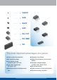
PhotoMOS technology
What makes PhotoMOS relays so successful?
Modern semiconductor technology ena-
bles fast, quiet, bounce-free switching,
even in miniature sizes. PhotoMOS relays
nevertheless enjoy an almost unlimited
lifetime if used according to the specifica-
tions. Moreover, they are extremely reli-
able, unaffected by vibrations, and their
ON-resistance remains stable throughout
their entire lifetime.
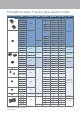
The basic construction of the PhotoMOS
relay can be seen in the illustration. Light
emitted from an LED on the input side pas-
ses through an isolator permeable to light
and is detected by a solar cell. Via a trigger
circuit, the solar cell's output voltage
controls the gates of two source-coupled
MOSFETs at the output. This arrangement
allows PhotoMOS relays to switch both AC
and DC loads.
The integration of MOSFET technology in
PhotoMOS relays differentiate them sig-
nificantly from semiconductor relays with
triacs or transistors at the output.
Output
LED
Input
2 x
MOSFET
Isolator
Photoelement
with DIC
Light