
Datasheet


Design, Specifications are subject to change without notice. Ask factory for technical specifications before purchase and/or use.
Whenever a doubt about safety arises from this product, please inform us immediately for technical consultation without fail.
−FC16−
Plastic Film Capacitors
Stacked Metallized PPS Film Chip Capacitor
Type: ECHU(X)
Stacked metallized PPS film as dielectric with simple
mold-less construction
■Features
•
Small in size (minimum size 1.6 mm
✕
0.8 mm)
•
85 ˚C, 85 %RH, W.V.
✕
1.0 for 500 hours
•
For reflow soldering
•
RoHS directive compliant
■Recommended Applications
•
Time-constant
•
Filtering
•
Oscillation and resonance
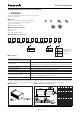
■Explanation of Part Numbers
123456789101112
E C H U
Product code
Dielectric &
construction
Rated voltage
Capacitance
X
Cap. Tol. Suffix
Suffix
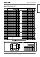
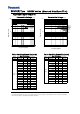
■Specifications
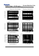
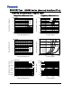
■Construction
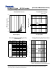
■Dimensions in mm (not to scale)
❈ Please consult us for flow soldering
❈
In case of applying voltage in alternating current (50 Hz or 60 Hz sine wave) to a capacitor with DC rated voltage, please
refer to the page of “Permissible voltage (R.M.S) in alternating current corresponding to DC rated voltage”.
1C 16 VDC
1H 50 VDC
5
8 mm
size ø180 mm
9
12 mm
size ø330 mm
❈
Tape width 8 mm
and diameter
ø330 mm reel is
prepared.
Tape width
Reel diameter
Category temp. range
(Including temperature-rise on unit surface)
Rated voltage
Capacitance range
Capacitance tolerance
Withstand voltage
Dissipation factor (tan )
Insulation resistance (IR)
−55 ℃ to +125 ℃
16 VDC,50 VDC
(50 VDC: 0.12 µF or more: Derating or rated voltage by 1.25 % / ℃at more than 105 ℃)
0.00010 µF to 0.22 µF (E12)
±
2 %(G),
±
5 %(J)
Between terminals : Rated volt. (VDC)
✕
150 % 60 s
tanδ≦0.6 % (20 ℃, 1 kHz)
16 VDC:IR≧3000 MΩ (20 ℃, 10 VDC, 60 s)
50 VDC:IR≧3000 MΩ (20 ℃, 50 VDC, 60 s)
Soldering conditions
Reflow soldering : 260 ˚C max. and 95 sec max. at more than 220 ˚C (Temp. at cap. surface)
saize
code
L WH e g
K1 1.6 0.8 0.7 0.35 ≧0.4
J1 2.0 1.25 0.9 0.45 ≧0.6
J2 2.0 1.25 1.1 0.45 ≧0.6
H1 3.2 1.6 0.9 0.65 ≧1.0
H2 3.2 1.6 1.1 0.65 ≧1.0
H3 3.2 1.6 1.5 0.65 ≧1.0
G1 3.2 2.5 1.1 0.65 ≧1.0
G2 3.2 2.5 1.5 0.65 ≧1.0
G3 3.2 2.5 2.1 0.65 ≧1.0
E1 4.8 3.3 1.5 0.80 ≧2.0
E2 4.8 3.3 2.1 0.80 ≧2.0
D1 6.0 4.1 1.9 0.80 ≧2.0
D3 6.0 4.1 2.5 0.80 ≧2.0
D4 6.0 4.1 2.8 0.80 ≧2.0
G
±
2 %
J
±
5 %
p Œ ¯ ¶ ‚ P1 ‘32 12.11.14 20:49 y [ W 16