
Datasheet

FIBER
SENSORS
LASER
SENSORS
PHOTO-
ELECTRIC
SENSORS
MICRO
PHOTO-
ELECTRIC
SENSORS
AREA
SENSORS
SAFETY
COMPONENTS
PRESSURE
SENSORS
INDUCTIVE
PROXIMITY
SENSORS
PARTICULAR
USE
SENSORS
SENSOR
OPTIONS
WIRE-
SAVING
SYSTEMS
MEASURE-
MENT
SENSORS
STATIC
CONTROL
DEVICES
LASER
MARKERS
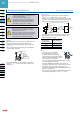
Selection
Guide
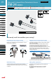
PM-24
PM-64
PM-44/54
U-shaped
Convergent
Reflective
PM2
PM-24
Ultra-small U-shaped Micro Photoelectric Sensor PM-24 SERIES
422
MICRO
PHOTO-
ELECTRIC
SENSORS
U-shaped
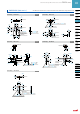
I/O CIRCUIT AND WIRING DIAGRAMS
PM-□24 PM-□24-R
NPN output type
I/O circuit diagram Wiring diagram
Notes: 1) Make sure to connect terminals correctly as the sensor does not
incorporate a reverse polarity protection circuit.
Further, the output is not incorporated with a short-circuit
protection circuit. Do not connect it directly to a power supply or a
capacitive load. Faulty wiring may result in damage.
2) Ensure to insulate the unused output wire.
Output operation
Color code
Output opera
tion
Output 1 Black Light-ON
Output 2 White Dark-ON
Symbols … Z
D1
, Z
D2
: Surge absorption zener diode
Tr
1
, Tr
2
: NPN output transistor
Color code
Sensor circuit
(Brown) +V
5 to 24 V DC
± 10 %
+
–
(Blue) 0 V
Users’ circuitInternal circuit
ZD1
ZD2
Tr2
Tr1
50 mA max.
50 mA max.
(Black) Output 1
(Note 1,2)
(White) Output 2 (Note 1,2)
Load
Load
Brown
5 to 24 V DC
± 10 %
+
–
Black
White
Blue
Load
Load
PM-□24P
PNP output type
I/O circuit diagram Wiring diagram
Output operation
Color code
Output operation
Output 1 Black Light-ON
Output 2 White Dark-ON
Color code
Sensor circuit
(Brown) +V
5 to 24 V DC
± 10 %
+
–
(Blue) 0 V
Users’ circuitInternal circuit
ZD1
ZD2
Tr2
Tr1
50 mA max.
50 mA max.
(Black) Output 1 (Note 1,2)
(White) Output 2 (Note 1,2)
Load
Load
Brown
5 to 24 V DC
± 10 %
+
–
Black
White
Blue
Load
Load
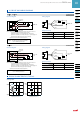
SENSING CHARACTERISTICS (TYPICAL)
Sensing position
Notes: 1) Make sure to connect terminals correctly as the sensor does not
incorporate a reverse polarity protection circuit.
Further, the output is not incorporated with a short-circuit
protection circuit. Do not connect it directly to a power supply or a
capacitive load. Faulty wiring may result in damage.
2) Ensure to insulate the unused output wire.
Symbols … Z
D1
, Z
D2
: Surge absorption zener diode
Tr
1
, Tr
2
: PNP output transistor
Dark-
ON
Light-
ON
Operating point ℓ (mm in)
ℓ
0 1
0.039
Beam
axis
2 mm
0.079 in
5.5 mm
0.217 in
2
0.079
3
0.118
4
0.157
Dark-
ON
Light-
ON
ℓ
0
6 mm
0.236 in
1
0.039
2
0.079
3
0.118
4
0.157
Operating point ℓ (mm in)