
Integration Guide


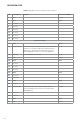
Table Of Contents
- Cover
- Table of Contents
- Tables and Figures
- Text Format Conventions
- Terms and Abbreviations
- Referenced Documents
- 1. Overview
- 2. Architecture
- 3. Connectors
- 4. Software Integration
- 5. Mechanical
- 6. Compliance
- 6.1. Manufacturer’s Federal Communication Commission (FCC) Compliance Statements
- 6.1.1. Antenna Information
- 6.1.2. FCC Declaration of Conformity Statement
- 6.1.3. FCC Radiation Exposure Statement
- 6.1.4. Factors Affecting Module Usage Related to FCC Compliance
- 6.2. Manufacturer’s Innovation, Science and Economic Development (ISED) Canada Compliance Statements
- 6.2.1. Antenna Information
- 6.2.2. ISED (Canada) Compliance Statement
- 6.2.3. ISED Canada Radiation Exposure Statement
- 6.2.4. Factors Affecting Module Usage Related to ISED Compliance
- 6.2.4. Limites d'utilisation du module liées à la conformité ISED
- 6.3. Manufacturer’s European Union (EU) and United Kingdom (UK) Compliance Statements
- 6.3.1. EU and UK Declaration of Conformity
- 6.3.2. Antenna Information
- 6.3.3. European Union and UK Radiation Exposure Statement
- 6.3.4. EU and UK Compliance Statement
- 7. Safety Notices
- Industrial IoT Product Usage

9
INTEGRATION GUIDE
Pin Description Legend Direction on Radio
1 WAKE# Open drain, active low signal. When the card supports
wakeup, this signal is used to request that the system
return from a sleep/suspended state to service a
function-intiated event.
Input/Output
3 COEX1 Chip Power down control. Connected to CHP_PWD_L
on the QCA 9898. Must be de-asserted after both 3.3
V power and 1.1 V power become stable.
5 Unused
7 CLKREQ# Reference clock request signal Output
9 GND GND
11 REFCLK- PCI Express dierential reference clock (100 MHz) Input
13 REFCLK+ PCI Express dierential reference clock (100 MHz) Input
15 GND GND
Mechanical Key
17 Unused
19 Unused
21 GND GND
23 PERn0 PCI Express Rx- (Rx WRT host) Output
25 PERp0 PCI Express Rx+ (Rx WRT host) Output
27 GND GND
29 GND GND
31 PETn0 PCI Express Tx- (Tx WRT host) Input
33 PETp0 PCI Express Tx+ (Tx WRT host) Input
35 GND GND
37 GND PCIe Lane 2 GND GND
39 Unused
41 Unused
43 GND PCIe Lane 2 GND GND
45 Reserved
47 Reserved
49 Reserved
51 Reserved
Table 1. Mini PCIe connector pinout for the odd pins