E‐14 Hardware Technical Reference Release: 14.1.8.12 Hardware Version: F Pico E14 Hardware Reference www.picocomputing.com (206) 283‐2178 Pico Computing, Inc. 150 Nickerson Street.
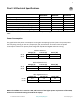
Contents: Product Overview Quick Reference Datasheet Electrical Specifications System Architecture 4 5 6 7 Features Field Programmable Gate Array Power‐PC™ Processor CPLD TurboLoader Tri‐Mode Ethernet Interface Flash Memory DDR2 Memory 8 9 10 11 12 13 I/O Interfaces Analog Interface RS‐232 Serial Interface Digital Peripheral Interface CardBus Interface Digital Bus Interface JTAG Debug Interface 14 15 16 17 18 19 Appendices A – Peripheral I/O Connector Information B – CardBus Connector Information C
Product Overview: The Pico families of product are revolutionary embedded platforms. With performance that often exceeds modern microcomputers, a shockingly small form factor, and nominal power consumption that is less than one watt, the Pico family of products takes computing to a whole new level. The Pico E‐14 is based on the revolutionary Virtex‐4 chip.
Pico E-14 EP Quick Reference Datasheet Core Technologies Features - Virtex-4 FPGA - PowerPC-405 450 MHz (680 DMIPS) - 256 MB RAM - 64 MB FPGA Image Flash - Analog to Digital and Digital to Analog Converters - Gigabit Ethernet (1000/100/10 Mbps) - 2 RS-232 Serial Ports - JTAG Hardware / Software Debugging - 54-bit High Speed Digital I/O Bus - 16-bit external digital I/O port - Standalone operation - JTAG hardware / software debugging - Open source Mechanical Specification - Cardbus Type II - Stainless
Pico E‐14 Electrical Specifications Minimum Nominal Maximum DC Input Voltage Power Consumption 3.15V 3.3‐5.0V 5.5V 10W* Recommended Temperature Range Maximum Allowable Temperature Range Continuous Storage Temperature Range Relative Humidity (Non‐Condensing) 0°C 0°C ‐50°C 0% 10°C 70°C 85°C 125°C 95% 30°C Note: If the card draws more than 10 watts the power supplies cut off and reset the card Power Consumption The graph below has power consumption running Pico Computing’s primary boot.
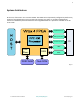
System Architecture At the core of the Pico E‐14 is a Virtex‐4 FPGA. The FPGA can be dynamically configured to perform any number of specialized tasks such as: protocol processing, encryption, or complex mathematical functions. Embedded systems benefit from the integrated Power‐PC™ processor available on the EP series cards. Gigabit Ethernet Analog Converters Serial Transceiver I/O JTAG DSP Slices DDR2 RAM RAM GPIO Flash ROM Figure 1 E‐14 Hardware Reference Manual www.picocomputing.
Field Programmable Gate Array The core of the Pico E‐14 is a high performance Virtex‐4 FPGA. Included in the FPGA are the FPGA Fabric, a Power‐PC ™ processor, ultra high‐speed DSP slices and DDR2 RAM. FPGA Fabric: The “Fabric” of an FPGA comprises an array of logic elements that can be connected in virtually unlimited patterns.
PowerPC™ Processor PPC405x3 Processor Introduction: FPGAs are renowned for their ability to process parallel logic, but they typically have a hard time emulating a high performance processor. To get the best of both worlds the Virtex‐4™ features an embedded Power PC Processor. Since the processor shares the same die as the FPGA it seamlessly interfaces with the FPGA fabric. A new feature of the Vitex‐4 FPGA is the addition of an auxiliary processor interface.
CPLD TurboLoader A CPLD (Complex Programmable Logic Device) is a smaller version of an FPGA (described above) with permanent Flash storage built in. The Pico E‐14 contains one CPLD that loads and reconfigures the FPGA. The Pico firmware guide describes how to access the CPLD Image Manager. CPLD Resources: Xilinx CPLD Website E‐14 Hardware Reference Manual www.xilinx.com/cpld www.picocomputing.com Pico Computing, Inc.
Tri‐Mode Ethernet Interface The Pico E‐14 features the Marvell Alaska series 88E1111 tri‐mode Ethernet transceiver. On EP series parts the MAC (Middle access controller) is implemented on the FPGA die. On LO series parts the MAC must be implemented in firmware. Communication between the MAC and PHY takes place over an industry standard MII/GMII interface. The Ethernet transceiver features 10/100/1000 full/half duplex operation.
Flash Memory The Pico E‐14 comes equipped with at least 64 megabytes of Flash ROM. The Flash ROM is divided into 512 sectors that can be erased independently. Most of the space on the ROM is reserved for the user. The Flash ROM’s address bus can be controlled by either the TurboLoader or the FPGA, but not both. During power‐up or reboot, the TurboLoader is in control of the Flash ROM Address bus. At all other times the FPGA is in control of the address bus.
DDR2 Memory The Pico E‐14 comes equipped with 256 MB of PC‐266 DDR2 memory. There are four 256Mb chips each with 16 bit data paths that are grouped into two 32 bit banks. From 0°C to +95°C, the ram can run at 266 MHz. For operation at temperatures below 0°C, special firmware with reduced ram timings is required. The temperature compensated self‐refresh mode must be disabled below ‐20°C.
Analog Interface (Optional) The Pico E‐14 also comes equipped with two high‐speed analog converters each capable of 14‐bit resolution. By default, both analog converters are powered down until the sleep lines are driven low and the amplifier lines are driven high by the FPGA. Both converters are capacitively coupled with pull‐ down resistors on the output to filter out any DC signal components. Both amplifiers are configured for minimum noise and unity gain.
*Please refer to the Analog Interface Selection Guide in Appendix E for compatible 8‐12‐bit converters RS‐232 Serial Transceiver The Pico E‐14 contains one asynchronous RS‐232 serial transceiver that also meets EIA/TIA‐232 and V.28/V.24 specifications at a maximum data rate of 250kBps. Because the serial transceiver is directly connected to the FPGA any bit high‐level protocol can be implemented in logic. Pico Computing supports various asynchronous, synchronous and military serial protocols.
Digital Peripheral Interface The Pico E‐14 features 16 GPIO lines that are used for external peripheral support. Pulling the DIAG_EN pin low replaces 4 GPIO signals with JTAG signals. All GPIO signals have user selectable pull‐up, pull‐down, keeper or HI‐Z termination. Drive strength is also user selectable between 2 and 24mA. All GPIOs can be configured for input, output and bi‐ directional mode and are equipped with ESD protection.
CardBus Interface The Pico E‐14 can run as a standalone product or be connected to a host using the CardBus connector. By default, the Pico E‐14 ships with firmware that is ready for use as a CardBus slave device, but it also supports bus mastering. That same firmware also provides the means to switch into standlone mode.1 CardBus is a 32‐bit interface with a maximum speed of 33 MHz. The Pico E‐14 hardware is designed to support standard PCMCIA as well as DMA mode.
Digital Bus Interface When the Pico E‐14 is not connected to a CardBus host, the digital bus can be reconfigured to connect with a wide variety of high‐speed digital busses and peripherals. All signals have user selectable pull‐ up, pull‐down, keeper or HI‐Z termination. Drive strength is also user selectable between 2 and 24mA. All pins can be configured for input, output and bi‐directional mode. With proper termination, speeds of over 200 MHz are possible.
JTAG Debug Interface The Pico E‐14 is equipped with a JTAG diagnostic port that allows real‐time debugging of hardware, firmware and software. Use of the external JTAG port disables four external GPIO pins as well as the internal JTAG loop back. Some JTAG programs require the length of the instruction register (IR). The IR length is listed below for all devices in the JTAG chain.
Appendix A – Peripheral I/O Connector Information Connector Information Description Mating Connector Mating Connector Backshell Brand Hirose Hirose Part Number NX30TA‐32PAA(50) NX‐32TA‐CV1(50) *Connectors are always in stock at Pico Computing Peripheral I/O Connector Pinout 1 2 3 4 5 6 7 8 9 10 11 12 13 14 15 16 17 18 19 20 21 22 23 24 25 26 27 28 29 30 31 32 ETHER_OUT_DD‐ ETHER_OUT_DD+ GPIO_15_FILTERED GPIO_14_FILTERED GPIO_13_FILTERED GPIO_12_FILTERED ETHER_OUT_DC‐ ETHER_OUT_DC+ GPIO_11_FILTERED
Peripheral Connector Pin #1 Location Figure 5 Appendix B – CardBus Connector Information Connector Information Description CardBus Header Brand Hirose Part Number IC9‐68RD‐0.635SF‐(51) The Pico E‐14 will mate with any Type‐II CardBus Header The function and direction of the pins on the CardBus interface can be easily changed. Please see the “Digital Bus Interface” section for more information.
CAD26 CAD27 CAD29 RFU C\C\L\K\R\U\N\ GND GND C\C\D\1\ CAD2 CAD4 CAD6 RFU CAD8 CAD10 C\V\S\1\ CAD13 CAD15 CAD16 RFU C\B\L\O\C\K\ C\S\T\O\P\ C\D\E\V\S\E\L\ VCC VPP C\T\R\D\Y\ C\F\R\A\M\E\ CAD17 CAD19 C\V\S\2\ C\R\S\T\ C\S\E\R\R\ C\R\E\Q\ C\C\/\B\E\3\ CAUDIO CSTSCHG CAD28 CAD30 CAD31 C\C\D\2\ GND 29 30 31 32 33 34 35 36 37 38 39 40 41 42 43 44 45 46 47 48 49 50 51 52 53 54 55 56 57 58 59 60 61 62 63 64 65 66 67 68 CardBus Data/Address 26 CardBus Data/Address 27 CardBus Data/Address 29 Reserved For Future
E‐14 Hardware Reference Manual www.picocomputing.com Pico Computing, Inc.
Appendix C – FPGA Pinout FPGA Pinout 50MHZ_CLOCK 50MHZ_CLOCK 50MHZ_CLOCK 50MHZ_CLOCK 50MHZ_CLOCK 50MHZ_CLOCK ADC_AMP_PWUP ADC_CLK ADC_D0 ADC_D1 ADC_D2 ADC_D3 ADC_D4 ADC_D5 ADC_D6 ADC_D7 ADC_D8 ADC_D9 ADC_D10 ADC_D11 ADC_D12 ADC_D13 ADC_MODE ADC_OTR ADC_PDWN CB_CAD0 CB_CAD1 CB_CAD2 CB_CAD3 CB_CAD4 CB_CAD5 CB_CAD6 CB_CAD7 CB_CAD8 CB_CAD9 CB_CAD10 CB_CAD11 CB_CAD12 CB_CAD13 CB_CAD14 AA14 AB12 AB14 AC13 AD15 AE13 AD14 V23 W23 T24 V21 W18 Y22 W20 AB21 Y18 AB20 AC21 T20 R20 R21 V18 T17 T18 V22 K3 F3 D3 C3 M6
CB_CAD15 CB_CAD16 CB_CAD17 CB_CAD18 CB_CAD19 CB_CAD20 CB_CAD21 CB_CAD22 CB_CAD23 CB_CAD24 CB_CAD25 CB_CAD26 CB_CAD27 CB_CAD28 CB_CAD29 CB_CAD30 CB_CAD31 CB_CAUDIO CB_CBLOCK CB_CC/BE0 CB_CC/BE1 CB_CC/BE2 CB_CC/BE3 CB_CCLK CB_CCLKRUN CB_CDEVSEL CB_CFRAME CB_CGNT CB_CINT CB_CIRDY CB_CPAR CB_CPERR CB_CREQ CB_CRST CB_CSERR CB_CSTOP CB_CSTSCHG CB_CTRDY CB_RFU1 CB_RFU2 CB_RFU3 CPLD_TDI DAC_AMP_PWUP DAC_CLK DAC_CLK‐ DAC_CMODE D6 C7 J5 K6 E5 E6 E7 D9 C8 F10 G4 J3 L10 K8 F4 K11 H9 H3 B9 H4 C6 H6 D10 D11 G10 G12
DAC_D0 DAC_D1 DAC_D2 DAC_D3 DAC_D4 DAC_D5 DAC_D6 DAC_D7 DAC_D8 DAC_D9 DAC_D10 DAC_D11 DAC_D12 DAC_D13 DAC_MODE DAC_SLEEP ETHER_25MHZ ETHER_125MHZ ETHER_COL ETHER_COMA ETHER_CRS ETHER_IRQ ETHER_MDC ETHER_MDIO ETHER_RESET ETHER_RX0 ETHER_RX1 ETHER_RX2 ETHER_RX3 ETHER_RX4 ETHER_RX5 ETHER_RX6 ETHER_RX7 ETHER_RX_CLK ETHER_RX_CTL ETHER_RX_ER ETHER_TX0 ETHER_TX1 ETHER_TX2 ETHER_TX3 ETHER_TX4 ETHER_TX5 ETHER_TX6 ETHER_TX7 ETHER_TX_CLK ETHER_TX_CTL H16 K13 G11 J14 E10 H12 H13 C11 H14 G15 G14 J15 J16 G16 K10 E11
ETHER_TX_ER F\L\A\S\H\_\B\Y\T\E\ F\L\A\S\H\_\O\E\ F\L\A\S\H\_\R\E\S\E\T\ F\L\A\S\H\_\W\E\ F\L\A\S\H\_\W\P\ F\L\A\S\H\_C\E\ F\P\G\A\_\P\R\O FLASH_A0 FLASH_A1 FLASH_A2 FLASH_A3 FLASH_A4 FLASH_A5 FLASH_A6 FLASH_A7 FLASH_A8 FLASH_A9 FLASH_A10 FLASH_A11 FLASH_A12 FLASH_A13 FLASH_A14 FLASH_A15 FLASH_A16 FLASH_A17 FLASH_A18 FLASH_A19 FLASH_A20 FLASH_A21 FLASH_A22 FLASH_A23 FLASH_A24 FLASH_A25 FLASH_D0 FLASH_D1 FLASH_D2 FLASH_D3 FLASH_D4 FLASH_D5 FLASH_D6 FLASH_D7 FLASH_D8 FLASH_D9 FLASH_D10 FLASH_D11 AA18 AD3
FLASH_D12 FLASH_D13 FLASH_D14 FLASH_D15 FLASH_READY FPGA_CCLK FPGA_DONE FPGA_INIT GPIO_0 GPIO_1 GPIO_2 GPIO_3 GPIO_4 GPIO_5 GPIO_6 GPIO_7 GPIO_8 GPIO_9 GPIO_10 GPIO_11 GPIO_12 GPIO_13 GPIO_14 GPIO_15 JTAG_LOOP_TCK JTAG_LOOP_TDI JTAG_LOOP_TDO JTAG_LOOP_TMS LOAD PEEKABOO PIC_CLK PIC_DATA R\A\M\_\C\A\S\ R\A\M\_\C\L\K\ R\A\M\_\C\L\K\ R\A\M\_\C\S\0\ R\A\M\_\C\S\1\ R\A\M\_\R\A\S\ R\A\M\_\W\E\ RAM_A0 RAM_A1 RAM_A2 RAM_A3 RAM_A4 RAM_A5 RAM_A6 Y11 Y12 W16 V16 Y15 M14 K15 L15 AA4 AA5 AC22 AB22 Y5 W4 Y6 Y7 AB10 Y
RAM_A7 RAM_A8 RAM_A9 RAM_A10 RAM_A11 RAM_A12 RAM_BA0 RAM_BA1 RAM_CLK RAM_CLK RAM_CLKE0 RAM_CLKE1 RAM_D0 RAM_D1 RAM_D2 RAM_D3 RAM_D4 RAM_D5 RAM_D6 RAM_D7 RAM_D8 RAM_D9 RAM_D10 RAM_D11 RAM_D12 RAM_D13 RAM_D14 RAM_D15 RAM_D16 RAM_D17 RAM_D18 RAM_D19 RAM_D20 RAM_D21 RAM_D22 RAM_D23 RAM_D24 RAM_D25 RAM_D26 RAM_D27 RAM_D28 RAM_D29 RAM_D30 RAM_D31 RAM_DM0‐7 RAM_DM8‐15 E22 D24 F20 F23 A14 D23 E23 K18 C14 F15 A15 G22 C19 F18 G20 D19 C21 E20 F17 B17 D15 D14 C16 A17 G17 B16 C12 B12 H19 H22 G24 H24 J21 G19 K20 K23
RAM_DM16‐23 RAM_DM24‐31 RAM_LOOPBACK RAM_LOOPBACK RAM_ODT0 RAM_ODT1 RAM_STROBE0 RAM_STROBE1 RAM_STROBE2 RAM_STROBE3 RS232‐EN RS232‐RX RS232‐TX RS232‐VALID SLEEP TCK TDI TMS VRN1 VRN2 VRP1 VRP2 L18 N23 D13 H17 J19 D18 C18 C17 L23 K22 J13 M5 L5 L9 U4 U10 U11 T10 F14 J24 F13 H23 E‐14 Hardware Reference Manual Data Mask [16‐23] Data Mask [24‐31] Loopback Input Loopback Output On‐Die Termination Enable 0 On‐Die Termination Enable 1 Strobe D16‐D31 ‐ Bank 0 Strobe D0‐D15 ‐ Bank 0 Strobe D16‐D31 ‐ Bank 1 Str
Appendix D – CPLD Pinout CPLD Pinout Net Pin 50MHZ_CLOCK CPLD_TDI ETHER_TDI F\L\A\S\H\_\B\Y\T\E\ F\L\A\S\H\_\O\E\ F\L\A\S\H\_\R\E\S\E\T\ F\L\A\S\H\_\W\E\ F\L\A\S\H\_\W\P\ F\L\A\S\H\_C\E\ F\P\G\A\_\P\R\O\G\ FLASH_A0 FLASH_A1 FLASH_A2 FLASH_A3 FLASH_A4 FLASH_A5 FLASH_A6 FLASH_A7 FLASH_A8 FLASH_A9 FLASH_A10 FLASH_A11 FLASH_A12 FLASH_A13 FLASH_A14 FLASH_A15 FLASH_A16 FLASH_A17 FLASH_A18 FLASH_A19 FLASH_A20 FLASH_A21 FLASH_A22 FLASH_A23 FLASH_A24 FLASH_A25 FLASH_D15 FPGA_CCLK FPGA_DONE FPGA_INIT LOAD PEEKA
SLEEP C10 Sleep Mode Request I *Pin D15 turns into Address ‐1 when the Flash ROM is in 8 bit mode. E‐14 Hardware Reference Manual www.picocomputing.com Pico Computing, Inc.
Appendix E – Standard Part Number Listing Standard Part Number Listing Device Part Number Website XC4VFX20‐10FF672C XC4VFX60‐10FF672C XC2C64A‐7CP56I HYB18T512160BF‐3.7 S29GL512N10FAI010 88E1111‐B2‐BAB‐I000 AD9245ACP AD9744ACP ISL4221EIR http://www.xilinx.com/virtex4 Pico E‐14 EP FPGA CPLD RAM ROM Ethernet ADC DAC RS‐232 Serial E‐14 Hardware Reference Manual http://www.xilinx.com/cpld http://www.infineon.com http://www.amd.com/us‐en/FlashMemory http://www.marvell.com http://www.analog.
Appendix F – Errata The following section lists all known errata: All versions: Permanent damage will result if the Pico E‐14 is left un‐configured and powered on for more than 10 minutes. This should not be a problem since the Pico E‐14 automatically loads an FPGA image upon power‐on. E‐14 Hardware Reference Manual www.picocomputing.com Pico Computing, Inc.
Appendix G – FPGA Performance Enhancements Overview: Like most silicon devices, the FPGA on the Pico can be overclocked if proper cooling techniques are employed. Care must be taken to avoid thermal runaway. Thermal Runaway: As the die temperature of the FPGA increases, it draws more current. This extra current gets turned into heat. If thermal equilibrium is not reached with proper cooling, the FPGA will overheat or overstress the power supplies.
Appendix E – Analog Interface Selection Guide Parts in the table below are all pin‐compatible with footprints on the Pico E‐14 Card. Factors such as cost, power consumption, resolution, and speed should all be considered for the particular application in which the Pico E‐14 is utilized.
Revision History 14.1.8.11 Initial public release 14.1.8.12 Updated: Electrical Specifications, JTAG Debug interface, updated part numbers E‐14 Hardware Reference Manual www.picocomputing.com Pico Computing, Inc.
Legal Notices “Xilinx System Generator for DSP” is a registered trademark of Xilinx, INC. “Xilinx” and associated artwork are registered trademarks of Xilinx, INC. “Virtex” and associated artwork are registered trademarks of Xilinx, INC. “Virtex‐4” and associated artwork is registered trademarks of Xilinx, INC. “CoolRunner‐II” and associated artwork are registered trademarks of Xilinx, INC. “MATLAB” is a registered trademark of The MathWorks, INC.