Bluetooth Module HSBT3007- IA, HSBT3007- EA HANSONG (NANJING) TECHNOLOGY CO. , LTD. MANAGER CHECKED FILLED SO N G APROVED Customer. H A N S.
Revision control Date/Author Check by V1.0 Bruce/6.08.2020 V2.0 Bruce/7.13.2020 Approve by Remarks Add FCC Statement H A N SO N G Revision HSBT3007 module_datasheet CONFIDENTIAL 2 Version2.0– Jul. 13th HANSONG ( NANJING) TECHNOLOGY CO.
H A N SO N G 1 Pin view HSBT3007 module_datasheet CONFIDENTIAL 7 Version2.0– Jul. 13th HANSONG ( NANJING) TECHNOLOGY CO.
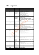
2 Pin Assignment Pin Name Description 1. GND GND Common Ground 2. AIO_0 Bidirectional Analog programmable input line 0 3. CS Bidirectional with weak pull-down Programmable input/output line 4. Alternative function: ■ SPI_CS#: chip select for Debug SPI, active low ■ I2S1_WS: I2S1 word select 4. MISO Bidirectional with weak pull-down Programmable input/output line 3. Alternative function: ■ SPI_MISO: Debug SPI data output ■ I2S1_SD_OUT: I2S1 synchronous data output 5.
enables the on-chip regulators VBAT 3.3V—4.2V GND 17. 3V3/1V8 Power in 3V3/1V8 TO Flash and IO VDD 18. 1.8V_SMPS Power out 1.8V_SMPS out 19. GND GND Common Ground 20. VBUS Power in Charger input. Typically connected to USB VBUS. 21. CHG_EXT output External battery charger transistor base control when using external charger boost. Otherwise leave unconnected. 22. VBAT_SENSE input Battery charger sense input. 23. USB_3.3V Power out USB_3.3V OUT 24.
PIO_21 Bidirectional with weak pull-down Programmable input/output line 21. 35. PIO_18 Bidirectional with weak pull-down Programmable input/output line 18. 36. LINE/MIC_AN Analog in Line or microphone input negative, channel A 37. LINE/MIC_AP Analog in Line or microphone input positive, channel A 38.
3 Interfaces 3.1 USB Interface HSBT3007 has a full-speed (12 Mbps) USB interface for communicating with other compatible digital devices. The USB interface on HSBT3007 acts as a USB peripheral, responding to requests from a master host controller. HSBT3007 contains internal USB termination resistors and requires no external resistors. HSBT3007 supports the Universal Serial Bus Specification, Revision v2.0 (USB v2.
3.3 SPI Interface HSBT3007 provides a debug SPI interface for programming, configuring (PS Keys) and debugging the HSBT3007. Access to this interface is required in production. Ensure the 4 SPI signals and the SPI/PCM# line are brought out to either test points or a header. To use the SPI A N SO N G interface, the SPI/PCM# line requires the option of being pulled high externally. H Noted:Pin to Pin distance is 1.27mm 3.
3.5 LED Drivers HSBT3007 includes a 3-pad PWM LED driver for driving RGB LEDs for producing a wide range of colors. All LEDs are controlled by application. The terminals are open-drain outputs, so the LED must be connected from a positive supply Figure 7-1 LED equivalent circuit SO N G rail to the pad in series with a current-limiting resistor. N From Figure 7-1 it is possible to derive Equation 7-1 to calculate ILED.
3.7 Reset HSBT3007 is reset from several sources: ■ RST# pin ■ Power-on reset ■ USB charger attach reset ■ Software configured watchdog timer The RST# pin is an active low reset and is internally filtered using the internal low frequency clock oscillator. Recommends applying RST# for a period >5ms. Automatic Reset Protection N 3.8 G At reset the digital I/O pins are set to inputs for bidirectional pins and outputs are set to tristate.
4 Battery Charger The battery charger hardware is controlled by the on-chip application. The battery charger has 5 modes: ■ Disabled ■ Trickle charge ■ Fast charge ■ Standby: fully charged or float charge ■ Error: charging input voltage, VCHG, is too low Transitions between the trickle charge, fast charge and standby modes are triggered by changes in battery voltage and charger current.
5 Power supply The system have two power supply mode: Mode1: Single 3.3V only supply. For improving the noise, recommend adding one 220Uf capacitor on the power supply SO N G pin If the HSBT3007 is powered with an external 3.3 V supply connected to the VBAT line, Power_EN must N be driven high after the IC has powered up otherwise the device may not initialise properly. Mode2. Single 5V only supply. the power.
6 General Specifications 6.1 Absolute Maximum Ratings: Ratings Min. Max. Unit Storage Temperature -40 +105 ℃ Supply Voltage (VBUS) -0.4 6.50 V Supply Voltage (POWER_EN) -0.4 4.40 V Supply Voltage (LED[2:0]) -0.4 4.40 V Supply Voltage (PIO_POWER) -0.4 3.60 V Typ G Max Unit -40 20 +85 ℃ SO 6.2 Recommended Operating Condition: 2.50 3.70 4.40 V 4.75/3.10 5.00 6.50 V 0 3.70 4.40 V - 3.70 4.40 V 1.70 1.80 3.
Trickle Charge Mode Min Unit Charge current Itrickle , as percentage of fast 8 10 12 V Vfast rising threshold - 2.9 - V Vfast rising threshold trim step size - 0.1 - V Vfast falling threshold - 2.8 - V charge current Fast Charge Mode Charge current during Maximum charge setting constant current mode, Ifast (VCHG - VBAT > 0.55 V) Minimum charge setting MIn Typ Max Unit 194 200 206 mA - 10 - mA 50 - 100 % - 10 - mA 4.16 4.20 4.24 V 4.31 4.35 4.
6.5 LED Driver Pads LED Driver Pads Min Typ Max Unit High impedance state - - 5 uA Current sink state - - 10 mA - - 0.55 V VOL output logic level low(a) - 0 - V VOH output logic level high(a) - 0.8 - V VIL input logic level low - 0 - V VIH input logic level high - 0.8 - V Current, IPAD LED pad voltage, VPAD IPAD = 10mA H A N SO N G (a) LED output port is open-drain and requires a pull-up HSBT3007 module_datasheet CONFIDENTIAL 19 Version2.0– Jul.
Layout Notes N SO N G 8 A. If there is battery, metal, LCD, loudspeaker, etc. beside the module antenna, it is required to A be at least 15mm away from the antenna B. It is recommended to use star routing for the power supply line during layout, and ensure available H that the power supply linearity of Bluetooth module is good, and the ground of BT is also It must be separated from the ground of operational amplifier, power amplifier, MCU, etc.
Dimension H A N SO N G 9 HSBT3007 module_datasheet CONFIDENTIAL 22 Version2.0– Jul. 13th HANSONG ( NANJING) TECHNOLOGY CO.
H A N SO N G 10 Reflow temperature HSBT3007 module_datasheet CONFIDENTIAL 23 Version2.0– Jul. 13th HANSONG ( NANJING) TECHNOLOGY CO.
11 FCC Statement This equipment has been tested and found to comply with the limits for a Class B digital device, pursuant to Part 15 of the FCC Rules. These limits are designed to provide reasonable protection against harmful interference in a residential installation. This equipment generate, uses and can radiate radio frequency energy and, if not installed and used in accordance with the instructions, may cause harmful interference to radio communications.
12 IC Statement This device complies with Industry Canada license-exempt RSS standard(s). Operation is subject to the following two conditions: (1) this device may not cause interference, and (2) this device must accept any interference, including interference that may cause undesired operation of the device. Caution: Modifications to this product will void the user’s authority to operate this equipment.
FR Language Le présent appareil est conforme aux CNR d’Industrie Canada applicables aux appareils radio exempts de licence. L’exploitation est autorisée aux deux conditions suivantes : (1) l’appareil ne doit pas produire de brouillage, et (2) l’utilisateur de l’appareil doit accepter tout brouillage radioélectrique subi, même si le brouillage est susceptible d’en compromettre le fonctionnement Caution: Les modifcations àce produit annuleront l'autoritéde l'utilisateur de faire fonctionner cet équipement.