User Manual RM3100 & RM2100 Geomagnetic Sensor
Table of Contents 1 2 3 4 5 COPYRIGHT & WARRANTY INFORMATION ............................................................ 3 INTRODUCTION .......................................................................................................... 4 SPECIFICATIONS ....................................................................................................... 5 3.1 GEOMAGNETIC SENSOR CHARACTERISTICS .......................................... 5 3.2 SEN-XY-F AND SEN-Z-F CHARACTERISTICS .................
List of Figures Figure 3-1: Figure 3-2: Figure 3-3: Figure 3-4: Figure 3-5: Figure 3-6: Figure 3-7: Figure 3-8: Figure 3-9: Figure 4-1: Figure 4-2: Figure 4-3: Figure 4-4: Figure 4-5: Figure 4-6: Figure 5-1: Sen-XY-f Sensor Dimensions ................................................................................ 8 Sen-XY-f Tape and Reel Dimensions .................................................................... 9 Sen-XY-f Recommended Solder Pad, Paste, & Mask Layout ...............................
1 Copyright & Warranty Information © Copyright PNI Sensor Corporation 2013 All Rights Reserved. Reproduction, adaptation, or translation without prior written permission is prohibited, except as allowed under copyright laws. Revised March 2014: for the most recent version visit our website at www.pnicorp.com PNI Sensor Corporation 2331 Circadian Way Santa Rosa, CA 95407, USA Tel: (707) 566-2260 Fax: (707) 566-2261 Warranty and Limitation of Liability.
2 Introduction Thank you for purchasing PNI Sensor Corporation’s RM2100 or RM3100 Geomagnetic Sensor, pn 90052 or pn 90053, respectively. The RM2100 is comprised of two Sen-XY-f sensor coils, pn 13104, and a MagI2C ASIC controller, pn 13156, which forms the basis for a 2-axis digital compass. The RM3100 is the same as the RM2100 but adds a Sen-Z-f sensor coil, pn 13101, such that compassing measurements are not constricted to the horizontal plane.
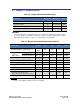
3 Specifications 3.1 Geomagnetic Sensor Characteristics Table 3-1: Geomagnetic Sensor Performance1 Parameter Field Measurement Range Cycle Counts2 50 100 200 Units -800 to +800 T 3 Gain 20 38 75 LSB/ T Sensitivity 50 26 13 nT Noise 30 20 15 nT Noise Density @ Max. Single-Axis Sample Rate Repeatability over 200 T 1.2 15 8 nT/ Hz 8 nT Hysteresis over 200 T 15 nT Linearity over 200 T 0.5 % Maximum Single-Axis Sample Rate (divide by 3 for max.
3.2 Sen-XY-f and Sen-Z-f Characteristics Table 3-2: Sen-XY-f and Sen-Z-f Absolute Maximum Ratings Parameter Minimum Maximum Units Input Pin Current @ 25 C 50 mA Voltage Across Coil 2.0 VDC +85 C Storage Temperature -40 CAUTION: Stresses beyond those listed above may cause permanent damage to the device. These are stress ratings only. Assuming operation with the MagI2C per the guidelines in this manual, these maximum ratings will not be violated.
3.3 MagI2C Characteristics Table 3-4: MagI2C Absolute Maximum Ratings Parameter Minimum Maximum Units Analog/Digital DC Supply Voltage, AVDD & DVDD -0.3 +3.7 VDC Input Pin Voltage -0.3 AVDD or DVDD VDC Input Pin Current @ 25C -10.0 +10.0 mA Storage Temperature -40° +125° C CAUTION: Stresses beyond those listed above may cause permanent damage to the device. These are stress ratings only.
3.4 Dimensions, Packaging, and Pad & Mask Layout 3.4.
Dimensions in mm Full reel is 5000 pcs. Smaller quantities on cut tape. Tape & reel meets ANSI/EIA standard EIA-418-B Figure 3-2: Sen-XY-f Tape and Reel Dimensions Note: PNI recommends a 5 mil stencil. The solder paste area is much smaller than the pad to reduce sensor tilt and misalignment. The above layout allows for rework: for minimal footprint, contact PNI.
3.4.
Dimensions in mm Full reel is 1200 pcs. Smaller quantities on cut tape. Tape & reel meets ANSI/EIA standard EIA-418-B Figure 3-5: Sen-Z-f Tape and Reel Dimensions Note: PNI recommends a 5 mil stencil. The solder paste area is much smaller than the pad to reduce sensor tilt and misalignment. The above layout allows for rework: for minimal footprint, contact PNI.
3.4.
Dimensions: mm Full reel is 5000 pcs. Smaller quantities on cut-tape. Tape & Reel meets ANSI/EIA standard EIA-418 Figure 3-8: MagI2C MLF Tape Dimensions 3.5 Soldering Figure 3-9 and Table 3-6 provide the recommended solder reflow profile and processing parameters for RM3100 components. After soldering PNI components to a board, it is possible to wave solder the opposite side of the PCB. IMPORTANT: PNI sensor coils require the use of halide-free solder pastes and processes for reflow and cleaning.
PB Figure 3-9: Recommended Solder Reflow Profile Table 3-6: Recommended Solder Processing Parameters1 Parameter Symbol Value Preheat Temperature, Minimum TSmin 150°C Preheat Temperature, Maximum TSmax 200°C 60 – 180 seconds Preheat Time (TSmin to TSmax) Solder Melt Temperature TL Ramp-Up Rate (TSmax to TL) Peak Temperature >218°C 3°C/second maximum TP Time from 25°C to Peak (TP) <260°C 6 minutes maximum Time above TL tL 60 – 120 seconds Soak Time (within 5°C of TP) tP 10 – 20 seconds
4 Geomagnetic Sensor Overview & Set-Up 4.1 Overview Figure 4-1 and Figure 4-2 provide basic schematics for implementing the RM3100 Sensor Suite when using the SPI interface and I2C interface, respectively. The MagI2C is at the center of the schematic, as it ties the user’s host controller, on the left, to the three sensor coils, on the right. Unused sensor connections should remain floating.
Figure 4-2: RM3100 reference schematic – I2C Configuration A Sen-XY-f or Sen-Z-f sensor coil serves as the inductive element in a simple LR relaxation oscillation circuit which is composed of an external bias resistor along with digital gates and a comparator internal to the MagI2C. The coil’s inductance is a function of the magnetic field strength. As such, the frequency of oscillation of the circuit varies with the strength of the total magnetic field parallel to the sensor.
Because: the total magnetic field represents the sum of the local field and the circuit-induced field, and the circuit-induced magnetic field has the same magnitude but opposite direction for the two bias polarities, the local magnetic field is proportional to the difference in the time to complete the measurement for each bias.
Figure 4-4: RM3100 North-East-Down (NED) Sensor Layout If the Sen-Z-f sensor coil is flipped to the bottom of the board such that the polarity indicator still points back or the curved portion of the sensor still points forward, then to retain NED the Sen-Z-f’s ZDRVN and ZDRVP pads should be as shown above, except on the bottom of the board. As the pads on the Sen-Z-f have switched positions, the connections to the Sen-Z-f sensor will be reversed. 4.2.
If an RM3100 Evaluation Board is not available, gradually bring the component in question closer to one of the sensor coils and observe when the sensor reading from the MagI2C starts to change. 4.2.3 Other Layout Considerations Other design considerations include: To minimize the effect of gradients in the magnetic field, position the sensor coils as close to each other as possible.
Table 4-1: MagI2C Pin Assignments Pin# Pin Name Description 1 MOSI / SDA 2 RES Reserved – connect to ground 3 SSN / SA0 SPI interface – Active low to select port 2 I C interface – Bit 0 of MagI2C’s slave address 4 AVDD Supply voltage for analog section of ASIC 5 AVSS Ground pin for analog section of ASIC 6 ZDRVP Z sensor drive output 7 ZINP Z sensor measurement input 8 ZINN Z sensor measurement input 9 ZDRVN Z sensor drive output 10 YDRVP Y sensor drive output 11 YINP Y se
Sensor Drive and Measurement Pins (pins 6 – 13 & 15 – 18) The various sensor drive and measurement pins should be connected to the sensor coils. For a north-east-down (NED) reference frame, the connections should be as defined in Figure 4-4. I2CEN (pin 22) This pin should be pulled LOW when using the SPI interface or pulled HIGH when using the I2C interface. DRDY (pin 23) DRDY is used to ensure data is read from the MagI2C only when it is available.
After communication between the MagI2C and master device is finished, the SPI bus can be freed up (SSN pin set HIGH) to communicate with other slave devices while the MagI2C takes a measurement or is idle. SCLK (pin 27) SCLK is a SPI input used to synchronize the data sent in and out through the MISO and MOSI pins. SCLK is generated by the customer-supplied master device and should be 1 MHz or less. One byte of data is exchanged over eight clock cycles.
SA0 (pin 28) SA0 represents the least significant bit in the MagI2C’s slave address. Pulling this HIGH represents a ‘1’ and pulling it low represents a ‘0’. Along with pin 3 (bit 1) and the higher 5 bits (0b01000), which are pre-defined in hardware, SA0 establishes the 7-bit slave address of the MagI2C on the I2C bus. 4.4 SPI Timing Requirements The MagI2C can act as a slave device on a SPI bus. The SPI interface consists of four signals, as carried on SCLK, MOSI, MISO, and SSN.
Figure 4-5: SPI Timing Diagram, CPOL = CPHA = 0 Figure 4-6: SPI Timing Diagram, CPOL = CPHA = 1 PNI Sensor Corporation RM3100 & RM2100 Sensor Suite User Manual Doc 1017252 r03 Page 24 of 45
Table 4-2: SPI Timing Specifications Symbol Description Min Max Units tSHZD SSN LOW to data output 100 ns tSSDV SSN LOW to Command Byte 100 ns tDBSH Setup data before active edge 50 ns tDASH Hold data after active edge 50 ns tDRDV Clock falling edge to valid data tSSH Final clock cycle falling edge to SSN HIGH tSHDZ SSN HIGH to output data tri-state tSSW SSN HIGH to LOW (time between transactions) 10 100 ns ns 100 ns 100 4.
All communication is on the SDA line. The transaction is initiated by the host, or master, sending the Start condition followed by the MagI2C’s slave address, and then the RW bit is set to ‘0’, indicating a Write operation. The slave address is acknowledged by the MagI2C by setting SDA to LOW. This is followed by the desired 7-bit register address and then the register data. The register value automatically increments after every received data byte.
5 MagI2C Operation The primary functions of the MagI2C are: Set the Cycle Count Registers if the default is not desired. Initiate either a Single Measurement or Continuous Measurement. Confirm New Data Ready. Read the Measurement Results Registers. Each of these steps is discussed in detail in the following sections. Note: The MagI2C incorporates an Idle Mode to reduce power consumption. The device automatically idles when not exchanging data or taking a measurement.
5.1 Set the Cycle Count Registers (0x04 – 0x09) The Cycle Count Registers establish the number of sensor oscillation cycles (cycle counts) that will be counted for each sensor in both the forward and reverse bias directions during a measurement sequence. Each sensor has its own cycle count value, and each can be different. Increasing the cycle count value increases measurement gain and resolution.
5.2 Initiate Continuous Measurement Mode (0x01) The MagI2C can either take measurements automatically on a regular frequency (Continuous Measurement Mode) or by polling for single measurement. This section discusses Continuous Measurement Mode. See Section 5.3 for polling a single measurement. To initiate Continuous Measurement Mode, write to the CMM register address, 0x01, followed by the CMM register contents. To set the rate of data acquisition in Continuous Measurement Mode, see Section 5.2.1.
Table 5-3: Continuous Mode DRDY Options DRDY Requirements DRDM1 DRDM0 DRDY to HIGH when ALARM = 1, AND a full measurement sequence is completed, as established by CMX, CMY, and CMZ. 0 0 DRDY to HIGH after the completion of a measurement on any axis. 0 1 DRDY to HIGH after a full measurement sequence is completed, as established by CMX, CMY, and CMZ. 1 0 DRDY to HIGH when Alarm = 1.
To set the TMRC register, send the register address, 0x0B, followed by the desired TMRC register value. To read the TMRC register, send 0x8B. Note: The Cycle Count Registers establish the maximum data rate of the sensors. For instance, if the cycle count is set to 200D, then the maximum 3-axis update rate is ~430 Hz. If TMRC is set to 0x92, indicating an update rate of ~600 Hz, the rate established by the cycle count will override the TMRC request, and the actual update rate will be ~430 Hz.
There are two types of limits, Absolute and Relative. The LDM bit in the CMM register establishes which type will be used, where “0” indicates Absolute and “1” indicates Relative. In Absolute Alarm Mode, the limits are fixed and do not change, while in Relative Alarm Mode the limits change whenever the current Alarm Limits are exceeded. As the name suggests, Absolute Alarm Mode is used for monitoring the absolute magnetic field, while Relative Alarm Mode is used to monitor changes in magnetic field.
Since the registers are adjacent, it is not necessary to send multiple register addresses, as the MagI2C automatically will read/write to the next adjacent register. Relative Alarm Mode In Relative Alarm Mode the limits for each axis initially are set by the Alarm Lower Limit and Alarm Upper Limit value registers, as given in Table 5-5, similar to Absolute Alarm Mode. However, when the ALARM bit is triggered and set HIGH, the limit values are changed using the Alarm Hysteresis Values, given in Table 5-6.
case only the X axis sensor is being monitored, the ALLX register is set to 0x0A00, the AULX register is set to 0x1000, and the ADLX register is set to 0x0100. Table 5-7: Absolute vs.
5.4 Confirm New Data Ready There are several ways to determine if a measurement has been completed and data is available in the Measurement Results Registers. One method is monitoring the DRDY line for it to go HIGH. Recall that for continuous measurement mode, the DRDM bits of the Continuous Measurement Command byte establish the conditions for DRDY to go HIGH. Another option when using the SPI interface is monitoring the MISO pin for it to go HIGH.
Table 5-8: Measurement Results Registers Write Address (Hex) Read Address (Hex) X Axis Measurement (2) 24 A4 X Axis Measurement (1) 25 A5 X Axis Measurement (0) 26 A6 Y Axis Measurement (2) 27 A7 Y Axis Measurement (1) 28 A8 Y Axis Measurement (0) 29 A9 Z Axis Measurement (2) 2A AA Z Axis Measurement (1) 2B AB Z Axis Measurement (0) 2C AC Register Description Normally it is only necessary to send “A4H”, since the register value automatically increments on the clock cycles such
Where: STE – Setting this to ‘1’ commands the MagI2C to run the built-in self test when the POLL register is written to. The end of the built-in self test sequence will be indicated by DRDY going HIGH. ZOK, YOK, and XOK – These read-only bits indicate whether or not the X, Y, and Z LR oscillators functioned correctly during the built-in self test. A ‘1’ indicates a properly function oscillator. Note that STE also should be HIGH when this is read, or the reading is invalid.
Bit # 7 Value 0 6 5 4 NACK2 NACK1 NACK0 3 2 1 0 1 0 DRC1 DRC0 Where: DRC0 – Setting this to ‘1’ means DRDY is cleared by any device register write. Clearing occurs during reception of the register address byte for the write transaction on either the SPI or I2C interface. This is the default setting. DRC1 – Setting this to ‘1’ means DRDY is cleared by reading the Measurement Results registers. Clearing occurs when the MagI2C sends back the first byte of data. This is the default setting.
5.7.2 Making and Reading Measurements Figure 5-1 gives the SPI activity sequence for initiating a single measurement and reading the results. The MagI2C works for either CPOL=CPHA=0 or CPOL=CPHA=1, so both cases are given. The assumption in the diagram is that the DRDY pin or the MISO line is used to establish when data is ready, but a query of the Status Register could be used instead. SPI timing requirements are discussed in Section 4.4.
The steps to make measurements in Continuous Measurement Mode are given below. Start with SSN set HIGH, then set SSN to LOW. Initiate Continuous Measurement Mode by writing to the CMM register address, 0x01, followed by the CMM register value. This value defines which axes are to be measured, how the DRDY line will be set HIGH, and which type of Alarm will be implemented assuming the Alarm feature is being utilized.
Once the measurement sequence is completed on all desired axes, the DRDY pin is set HIGH and the MISO pin goes low, indicating data is read. The MagI2C is placed in Idle Mode. When the host is ready to read the measured values, set SSN to LOW. If SSN already is LOW, then toggle SSN from LOW to HIGH to LOW. Assuming the X axis was one of the axes to be measured, send the MX2 Read address, 0xA4, to begin reading the Measurement Results registers.
5.8.2 Initiate a Single Measurement The I2C transactions to initiate a single measurement on all 3 axes are given below. START S MagI2C ADDRESS 0 1 0 0 RW ACK POLL REG. ADDRESS (N) ACK 0 X X 0 0 0 0 0 0 0 0 0 0 0 DATA TO POLL REG (N) 0 1 1 1 0 0 0 ACK STOP 0 0 P From Host to MagI2C From MagI2C to Host After this transaction sequence the MagI2C will initiate a measurement sequence, and this can run in the background.
START S MagI2C ADDRESS 0 1 0 0 0 X RW ACK X 1 0 DATA FROM MX2 (N) X X X X X X ACK X X 0 DATA FROM MX1 (N+1) X X X X X X X ACK X 0 DATA FROM MX0 REG (N+2) ACK DATA FROM MY2 REG (N+3) ACK DATA FROM MY1 REG (N+4) ACK DATA FROM MY0 REG (N+5) ACK X X X X X X X X 0 X X X X X X X X 0 X X X X X X X X 0 X X X X X X X X DATA FROM MZ2 REG (N+6) ACK DATA FROM MZ1 REG (N+7) ACK DATA FROM MZ0 REG (N+8) NACK STOP X X X X X X X X 0 X X X X X X X X 0 X X X X X X X