
GP2Y0D810Z0F datasheet


GP2Y0D810Z0F
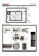
■Block diagram
■Outline Dimensions
(Unit : mm)
Product mass : approx. 0.7g
Signal
processing circuit
Distance measuring IC
V
PD
LED
LED drive circuit
Output circuit
Oscillation circuit
Voltage regulator
①
Cathode
LED_FB
②
LED
③
GND
④
REG
⑦
V
CC
V
CC
⑪
⑬
V
O
⑭
Anode
C
1
C
2
R
1
⑫
V
in
R1 (LED current adjustment resistance = 4.3 Ω) (LED Pulse current Typ. 70 mA)
C
1·C2=0.1μF
Stamp (Example)
14
(terminal root)
(terminal root)
Light emitter
Light detector
S 8 1 0
U 4 0 0 1
A
B
C
13
12
11
10
9
8
7
6
5
4
3
2
1
6.5
7.95
4.7
3
P1.5-5
0.2
0.40
2.5
13.6
7
6.2
(3°)
(3°)
year
2006
U
Mark
2007
V
2008
W
2009
X
2025
T
2026
U
....
....
DIN Standard year production
(Remove G, I, O, Q, Y, Z)
(It repeats itself by a period for 20 years)
D
S
U 4 0 0 1
8 1 0
SHARP「S」
GP2Y0D810Z0F
Month(1 to 9‚ O, N, D)
(DIN Standard symbol)
Year(DIN Standard symbol)
LOT No.
Material
Case
Lens
Device coating
Lead pin
PC (Color:Black)
PC(Visible light cut type)
PPS(Color:Black)
42ALLOY(Pd-Au plating)
A
B
C
D
Symbol
①
Cathode
②
LED_FB
③
LED
④
GND
⑤―
⑥―
⑦REG
⑧―
⑨―
⑩―
⑪
V
CC
⑫
V
in
⑬
V
O
⑭
Anode
(Note1) Unspecified tolerances shall be ±0.3mm.
(Note2) ( ) : Reference value
ー : No contact
Sheet No.: E4-A01101EN
2