
Data Sheet


DMOS Microstepping Driver with Translator
and Overcurrent Protection
A4988
12
Allegro MicroSystems, Inc.
115 Northeast Cutoff
Worcester, Massachusetts 01615-0036 U.S.A.
1.508.853.5000; www.allegromicro.com
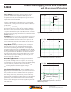
Application Layout
Layout. The printed circuit board should use a heavy ground-
plane. For optimum electrical and thermal performance, the
A4988 must be soldered directly onto the board. Pins 3 and 18
are internally fused, which provides a path for enhanced thermal
dissipation. Theses pins should be soldered directly to an exposed
surface on the PCB that connects to thermal vias are used to
transfer heat to other layers of the PCB.
In order to minimize the effects of ground bounce and offset
issues, it is important to have a low impedance single-point
ground, known as a star ground, located very close to the device.
By making the connection between the pad and the ground plane
directly under the A4988, that area becomes an ideal location for
a star ground point. A low impedance ground will prevent ground
bounce during high current operation and ensure that the supply
voltage remains stable at the input terminal.
The two input capacitors should be placed in parallel, and as
close to the device supply pins as possible. The ceramic capaci-
tor (CIN1) should be closer to the pins than the bulk capacitor
(CIN2). This is necessary because the ceramic capacitor will be
responsible for delivering the high frequency current components.
The sense resistors, RSx , should have a very low impedance
path to ground, because they must carry a large current while
supporting very accurate voltage measurements by the current
sense comparators. Long ground traces will cause additional
voltage drops, adversely affecting the ability of the comparators
to accurately measure the current in the windings. The SENSEx
pins have very short traces to the RSx resistors and very thick,
low impedance traces directly to the star ground underneath the
device. If possible, there should be no other components on the
sense circuits.
V
BB
V
DD
1
PAD
A4988
C3
C6
R1
R2
R3
C1
C8
C2
C9C7
RS2RS1
R6
C4
OUT1B
NC
DIR
REF
STEP
VDD
OUT2B
ENABLE
CP1
CP2
VCP
NC
VREG
MS1
MS2
MS3
RESET
ROSC
SLEEP
VBB2
SENSE2
OUT2A
NC
OUT1A
SENSE1
VBB1
GND
GND
PCB
Thermal Vias
Trace (2 oz.)
Signal (1 oz.)
Ground (1 oz.)
Thermal (2 oz.)
Solder
A4988