
Data Sheet
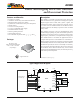

DMOS Microstepping Driver with Translator
and Overcurrent Protection
A4988
4
Allegro MicroSystems, Inc.
115 Northeast Cutoff
Worcester, Massachusetts 01615-0036 U.S.A.
1.508.853.5000; www.allegromicro.com
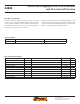
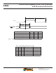
ELECTRICAL CHARACTERISTICS
1
at T
A
= 25°C, V
BB
= 35 V (unless otherwise noted)
Characteristics Symbol Test Conditions Min.
Typ.
2
Max. Units
Output Drivers
Load Supply Voltage Range V
BB
Operating 8 – 35 V
Logic Supply Voltage Range V
DD
Operating 3.0 – 5.5 V
Output On Resistance R
DSON
Source Driver, I
OUT
= –1.5 A – 320 430 m
Sink Driver, I
OUT
= 1.5 A – 320 430 m
Body Diode Forward Voltage V
F
Source Diode, I
F
= –1.5 A – – 1.2 V
Sink Diode, I
F
= 1.5 A – – 1.2 V
Motor Supply Current I
BB
f
PWM
< 50 kHz – – 4 mA
Operating, outputs disabled – – 2 mA
Logic Supply Current I
DD
f
PWM
< 50 kHz – – 8 mA
Outputs off – – 5 mA
Control Logic
Logic Input Voltage
V
IN(1)
V
DD
0.7
––V
V
IN(0)
––
V
DD
0.3
V
Logic Input Current
I
IN(1)
V
IN
= V
DD
0.7
–20 <1.0 20 A
I
IN(0)
V
IN
=
V
DD
0.3
–20 <1.0 20 A
Microstep Select
R
MS1
MS1 pin – 100 – k
R
MS2
MS2 pin – 50 – k
R
MS3
MS3 pin – 100 – k
Logic Input Hysteresis V
HYS(IN)
As a % of V
DD
51119%
Blank Time
t
BLANK
0.7 1 1.3 s
Fixed Off-Time
t
OFF
OSC = VDD or GND 20 30 40 s
R
OSC
= 25 k 23 30 37 s
Reference Input Voltage Range V
REF
0–4V
Reference Input Current I
REF
–3 0 3 A
Current Trip-Level Error
3
err
I
V
REF
= 2 V, %I
TripMAX
= 38.27% – – ±15 %
V
REF
= 2 V, %I
TripMAX
= 70.71% – – ±5 %
V
REF
= 2 V, %I
TripMAX
= 100.00% – – ±5 %
Crossover Dead Time t
DT
100 475 800 ns
Protection
Overcurrent Protection Threshold I
OCPST
2.1 – – A
Thermal Shutdown Temperature T
TSD
– 165 – °C
Thermal Shutdown Hysteresis T
TSDHYS
–15–°C
VDD Undervoltage Lockout V
DDUVLO
V
DD
rising 2.7 2.8 2.9 V
VDD Undervoltage Hysteresis V
DDUVLOHYS
–90–mV
1
For input and output current specifications, negative current is defined as coming out of (sourcing) the specified device pin.
2
Typical data are for initial design estimations only, and assume optimum manufacturing and application conditions. Performance may vary for individual
units, within the specified maximum and minimum limits.
3
V
ERR
= [(V
REF
/8) – V
SENSE
] / (V
REF
/8).