
Data Sheet

DMOS Microstepping Driver with Translator
and Overcurrent Protection
A4988
9
Allegro MicroSystems, Inc.
115 Northeast Cutoff
Worcester, Massachusetts 01615-0036 U.S.A.
1.508.853.5000; www.allegromicro.com
tion of current flow in each winding. The size of the increment is
determined by the combined state of the MSx inputs.
Direction Input (DIR). This determines the direction of rota-
tion of the motor. Changes to this input do not take effect until the
next STEP rising edge.
Internal PWM Current Control. Each full-bridge is con-
trolled by a fixed off-time PWM current control circuit that limits
the load current to a desired value, I
TRIP
. Initially, a diagonal pair
of source and sink FET outputs are enabled and current flows
through the motor winding and the current sense resistor, R
Sx
.
When the voltage across R
Sx
equals the DAC output voltage, the
current sense comparator resets the PWM latch. The latch then
turns off the appropriate source driver and initiates a fixed off
time decay mode
The maximum value of current limiting is set by the selection of
R
Sx
and the voltage at the VREF pin. The transconductance func-
tion is approximated by the maximum value of current limiting,
I
TripMAX
(A), which is set by
I
TripMAX
= V
REF
/ ( 8
R
S
)
where R
S
is the resistance of the sense resistor () and V
REF
is
the input voltage on the REF pin (V).
The DAC output reduces the V
REF
output to the current sense
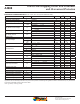
comparator in precise steps, such that
I
trip
= (%I
TripMAX
/ 100)
×
I
TripMAX
(See table 2 for %I
TripMAX
at each step.)
It is critical that the maximum rating (0.5 V) on the SENSE1 and
SENSE2 pins is not exceeded.
Fixed Off-Time. The internal PWM current control circuitry
uses a one-shot circuit to control the duration of time that the
DMOS FETs remain off. The off-time, t
OFF
, is determined by the
ROSC terminal. The ROSC terminal has three settings:
ROSC tied to VDD — off-time internally set to 30 s, decay
mode is automatic Mixed decay except when in full step where
decay mode is set to Slow decay
ROSC tied directly to ground — off-time internally set to
30 s, current decay is set to Mixed decay for both increasing
and decreasing currents, except in full step where decay mode
is set to Slow decay. (See Low Current Microstepping section.)
ROSC through a resistor to ground — off-time is determined
by the following formula, the decay mode is automatic Mixed
decay for all step modes.
t
OFF
R
OSC
⁄ 825
Where t
OFF
is in s.
Blanking. This function blanks the output of the current sense
comparators when the outputs are switched by the internal current
control circuitry. The comparator outputs are blanked to prevent
false overcurrent detection due to reverse recovery currents of the
clamp diodes, and switching transients related to the capacitance
of the load. The blank time, t
BLANK
(s), is approximately
t
BLANK
1 s
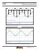
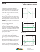
Shorted-Load and Short-to-Ground Protection.
If the motor leads are shorted together, or if one of the leads is
shorted to ground, the driver will protect itself by sensing the
overcurrent event and disabling the driver that is shorted, protect-
ing the device from damage. In the case of a short-to-ground, the
device will remain disabled (latched) until the S
¯
¯
L
¯
¯
E
¯
¯
E
¯
¯
P
¯
input goes
high or VDD power is removed. A short-to-ground overcurrent
event is shown in figure 4.
When the two outputs are shorted together, the current path is
through the sense resistor. After the blanking time (≈1 s) expires,
the sense resistor voltage is exceeding its trip value, due to the
overcurrent condition that exists. This causes the driver to go into
a fixed off-time cycle. After the fixed off-time expires the driver
turns on again and the process repeats. In this condition the driver
is completely protected against overcurrent events, but the short
is repetitive with a period equal to the fixed off-time of the driver.
This condition is shown in figure 5.
During a shorted load event it is normal to observe both a posi-
tive and negative current spike as shown in figure 3, due to the
direction change implemented by the Mixed decay feature. This
is shown in figure 6. In both instances the overcurrent circuitry is
protecting the driver and prevents damage to the device.
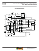
Charge Pump (CP1 and CP2). The charge pump is used to
generate a gate supply greater than that of VBB for driving the
source-side FET gates. A 0.1 F ceramic capacitor, should be
connected between CP1 and CP2. In addition, a 0.1 F ceramic
capacitor is required between VCP and VBB, to act as a reservoir
for operating the high-side FET gates.
Capacitor values should be Class 2 dielectric ±15% maximum,
or tolerance R, according to EIA (Electronic Industries Alliance)
specifications.