
Data Sheet

1
Wide V
IN
1A Synchronous Buck Regulator
ISL85410
The ISL85410 is a 1A synchronous buck regulator with an
input range of 3V to 36V. It provides an easy to use, high
efficiency low BOM count solution for a variety of applications.
The ISL85410 integrates both high-side and low-side NMOS
FETs and features a PFM mode for improved efficiency at light
loads. This feature can be disabled if a forced PWM mode is
desired. The part switches at a default frequency of 500kHz
but may also be programmed using an external resistor from
300kHz to 2MHz. The ISL85410 has the ability to utilize
internal or external compensation. By integrating both NMOS
devices and providing internal configuration options, minimal
external components are required, reducing BOM count and
complexity of design.
With the wide V
IN
range and reduced BOM, the part provides
an easy to implement design solution for a variety of
applications while giving superior performance. It will provide
a very robust design for high voltage industrial applications as
well as an efficient solution for battery powered applications.
The part is available in a small Pb-free 4mmx3mm DFN plastic
package with a full-range industrial temperature of -40°C to
+125°C.
Related Literature
• AN1905, “ISL85410EVAL1Z, ISL85418EVAL1Z Wide V
IN
1A,
800mA Synchronous Buck Regulator”
• AN1908
, “ISL85410DEMO1Z, ISL85418DEMO1Z Wide V
IN
1A, 800mA Synchronous Buck Regulator”
Features
• Wide input voltage range 3V to 36V
• Synchronous operation for high efficiency
• No compensation required
• Integrated high-side and low-side NMOS devices
• Selectable PFM or forced PWM mode at light loads
• Internal fixed (500kHz) or adjustable switching frequency
300kHz to 2MHz
• Continuous output current up to 1A
• Internal or external soft-start
• Minimal external components required
• Power-good and enable functions available
Applications
• Industrial control
•Medical devices
•Portable instrumentation
• Distributed power supplies
• Cloud infrastructure
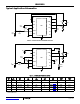
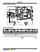
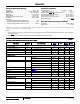
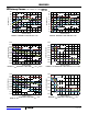
FIGURE 1. TYPICAL APPLICATION FIGURE 2. EFFICIENCY vs LOAD, PFM, V
OUT
= 3.3V
GND
C
BOOT
100nF
C
FB
R
3
R
2
PHASE
SS
SYNC
BOOT
VIN
PGND
FS
COMP
FB
VCC
PG
EN
C
VCC
1µF
C
VIN
10µF
L
1
22µH
1
2
3
4
5
6
9
10
11
12
INTERNAL DEFAULT PARAMETER SELECTION
C
OUT
10µF
V
OUT
50
55
60
65
70
75
80
85
90
95
100
V
IN
= 5V
V
IN
= 15V
V
IN
= 24V
V
IN
= 12V
V
IN
= 33V
OUTPUT LOAD (A)
EFFICIENCY (%)
0 0.10.20.30.40.50.60.70.80.91.0
CAUTION: These devices are sensitive to electrostatic discharge; follow proper IC Handling Procedures.
1-888-INTERSIL or 1-888-468-3774
| Copyright Intersil Americas LLC 2013, 2014. All Rights Reserved
Intersil (and design) is a trademark owned by Intersil Corporation or one of its subsidiaries.
All other trademarks mentioned are the property of their respective owners.
July 24, 2014
FN8375.5