TB67S279FTG Toshiba BiCD process integrated circuit silicon monolithic TB67S279FTG Active Gain Control Clock-in control Bipolar stepping motor driver The TB67S279FTG is a clock-in controlled bipolar stepping motor driver with a built-in Active Gain Control architecture. The TB67S279FTG also has an internal current feedback control (ACDS) which enables the driver to control the motor current without using a sense resistor. Using the BiCD process, the TB67S279FTG is rated at 50 V, 2.0 A. P-VQFN48-0707-0.
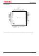
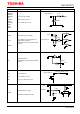
TB67S279FTG Pin assignment NC VMB VMB GND NC GND VREFB VREFA VCC VCC OSCM NC (Top View) 36 35 34 33 32 31 30 29 28 27 26 25 NC 37 24 OUTB+ NC 38 23 OUTB+ DMODE0 39 22 RSBGND DMODE1 40 21 RSBGND DMODE2 41 20 OUTB- CW/CCW 42 CLK 43 ENABLE 44 17 OUTA- 45 16 RSAGND MO 46 15 RSAGND LO1 47 14 OUTA+ LO2 48 13 OUTA+ 3 4 5 6 7 8 9 10 11 12 AGC1 CLIM1 FLIM BOOST LTH GND NC VMA NC 2 VMA 1 CLIM0 18 OUTA- AGC0 RESET 19 OUTB- TB67S279FTG Note: Please so
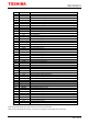
TB67S279FTG Pin description Pin No 1 2 3 4 5 6 7 8 9 10 11 12 13 14 15 16 17 18 19 20 21 22 23 24 25 26 27 28 29 30 31 32 33 34 35 36 37 38 39 40 41 42 43 44 45 46 47 48 Pin name AGC0 AGC1 CLIM0 CLIM1 FLIM BOOST LTH GND NC VMA VMA NC OUTA+ OUTA+ RSAGND RSAGND OUTAOUTAOUTBOUTBRSBGND RSBGND OUTB+ OUTB+ NC VMB VMB NC GND GND VREFB VREFA VCC VCC OSCM NC NC NC DMODE0 DMODE1 DMODE2 CW/CCW CLK ENABLE RESET MO LO1 LO2 Pin function Active Gain Control setup pin No.0 Active Gain Control setup pin No.
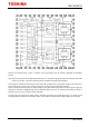
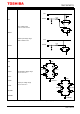
TB67S279FTG Block diagram Some of the functional blocks, circuits, or constants in the block diagram may be omitted or simplified for explanatory purpose. Note: All the grounding wires of the TB67S279FTG should run on the solder mask on the PCB and be externally terminated at only one point. Also, a grounding method should be considered for efficient heat dissipation.
TB67S279FTG Input-Output equivalent circuit Pin name DMODE0 DMODE1 DMODE2 CLK ENABLE RESET CW/CCW AGC0 AGC1 CLIM0 CLIM1 FLIM Input-Output signal Input-Output equivalent circuit Logic input pin 1 kΩ Logic input pin voltage GND ≤ VIN1 (L) ≤ 0.8 V 100 kΩ 2.0 V ≤ VIN1 (H) ≤ 5.5 V GND VCC Multi state input pin voltage 100 kΩ VCC, GND, VCC-100 kΩ pull-up, or GND-100 kΩ pull-down (Resistance accuracy should be within ±20 %.
TB67S279FTG Pin name Input-Output signal Input-Output equivalent circuit VCC 1 kΩ VREFA VCC VCC voltage range 4.75 V ≤ VCC ≤ 5.25 V VREFA VREF input voltage range GND ≤ VREF ≤ 3.6 V VCC 1 kΩ VREFB VREFB VMA VMA VMB OUT A+ OUTA+ VM operation voltage range 10 V ≤ VM ≤ 47 V OUTA- OUT AVMB RSAGND OUT B+ Output pin voltage range 10 V ≤ VM ≤ 47 V OUT B- OUTB- OUTB+ RSAGND RSBGND RSBGND Note: The equivalent circuit diagrams may be simplified or omitted for explanatory purposes.
TB67S279FTG ♦Basic function of stepping motor control 1. CLK function Each up-edge of the CLK signal shifts the current step and electrical angle of the motor. Note: Analog filter of 200 ns (±20 %) is adopted to CLK pin in the IC CLK Function ↑ Shifts the electrical angle and current step per each up-edge. ↓ — (no change, maintain former state) 2. ENABLE function The ENABLE pin controls the ON and OFF of the stepping motor outputs.
TB67S279FTG 5. RESET function The RESET pin initializes the internal electrical angle. Note: Built-in digital filter of 0.625 μs (±20 %) is adopted to RESET pin. RESET Function High Initializes the internal electrical angle Low Normal operation When the RESET pin is set to High, the current setting for each H-bridge (Ach and Bch) will be set to the value below. Also, the MO pin outputs Low level when the electrical angle corresponds to the initial value.
TB67S279FTG Step resolution and set current (Electric angle: 0 to 180°) Electrical angle 0° 45° 90° 135° 180° STEP 1/32 step 1/16 step 1/8 step 1/4 step 1/2(b) step 1/2(a) step 1 IOUTA(%) IOUTB(%) +100 0 ✔ ✔ ✔ ✔ ✔ ✔ 2 +100 +5 ✔ 3 +100 +10 ✔ 4 +99 +15 ✔ 5 +98 +20 ✔ 6 +97 +25 ✔ 7 +96 +29 ✔ 8 +94 +34 ✔ ✔ (Note1) ✔ ✔ ✔ (Note1) ✔ ✔ 9 +92 +38 ✔ 10 +90 +43 ✔ 11 +88 +47 ✔ 12 +86 +52 ✔ 13 +83 +56 ✔ 14 +80 +60 ✔ 15 +77 +63 ✔ 16 +74
TB67S279FTG Step resolution and set current (Electric angle: 180 to 360°) Electrical angle 180° 225° 270° 315° 360° STEP 1/32 step 1/16 step 1/8 step 1/4 step 1/2(b) step 1/2(a) step 65 IOUTA(%) IOUTB(%) -100 0 ✔ ✔ ✔ ✔ ✔ ✔ 66 -100 -5 ✔ 67 -100 -10 ✔ 68 -99 -15 ✔ 69 -98 -20 ✔ 70 -97 -25 ✔ 71 -96 -29 ✔ 72 -94 -34 ✔ 73 -92 -38 ✔ 74 -90 -43 ✔ 75 -88 -47 ✔ 76 -86 -52 ✔ 77 -83 -56 ✔ 78 -80 -60 ✔ 79 -77 -63 ✔ 80 -74 -67 ✔ ✔ (Note1) ✔
TB67S279FTG 7. LO1, LO2 (Error Output: error detect flag output) function The LO1 and LO2 are signals that are flagged when the error state is detected. Both pins are open drain type, therefore to use the function properly; the LO1 and LO2 pins should be pulled up to the VCC. (Set the pull-up resistor in the range of 10k to 100kΩ.) During normal operation, the pin is high-impedance (Internal MOSFET is turned off and the pin voltage is VCC).
TB67S279FTG OSCM oscillator frequency (chopping frequency) calculation OSCM oscillator frequency can be calculated by using the external component values (ROSC and COSC), and the formula is shown below. (COSC is fixed to 270 pF.) fOSCM = 4.0 x ROSC (-0.8) COSC and ROSC are external components to set the oscillator frequency. When adjusting the oscillator frequency with components, it is recommended to fix COSC to 270 pF and change the constant number of ROSC.
TB67S279FTG ♦Stepping motor application features (anti-stall, sense resistor less PWM) 9. Active Gain Control (Anti-stall) function AGC0, AGC1 pins control the Active Gain Control to turn on or off. When both pins are set to High, the AGC is turned on. The PWM current threshold will be reduced in a phased manner where the upper limited current is determined by VREF. When both pins are set to Low, the AGC is turned off and the current, which is set by VREF, flows. Note: Built-in digital filter of 0.
TB67S279FTG 12. FLIM (AGC Frequency limit) function The FLIM pin sets the bottom frequency limit for the AGC to be active. It can reduce the resonance frequency of the motor start in using AGC. The FLIM pin is a 4 stated logic input. Note: Built-in digital filter of 0.625 μs (±20%) is adopted to FLIM pin.
TB67S279FTG 14. ADMD + ACDS (sense-resistor less PWM) control ADMD (Advanced Dynamic Mixed Decay) The TB67S279FTG applied the ADMD architecture which monitors both charge and recirculating current during constant current PWM. The basic sequence of the ADMD is as shown below. fchop (=1/16 fOSCM) NFth fOSCM IOUT ADMDth Charge Fast Decay Slow Decay Mixed (Fast+Slow) Decay Timing charts may be simplified for explanatory purpose.
TB67S279FTG Constant current threshold calculation The constant current PWM threshold can be set by applying voltage to the VREF pin. IOUT=VREF × 0.556 Example: When Current Ratio is 100 % and VREF voltage is 2.0 V, the constant current PWM threshold is calculated from following formula. IOUT = 2.0 × 0.556=1.
TB67S279FTG • When the next current step/ratio is lower than the previous step fchop fchop fchop fchop Internal OSC waveform NFth ADMDth NF Charge NF Fast Charge Fast NF Slow Charge Slow Fast The current is charged for a short period of time to be compared in the RS comparator circuit. Since the motor current level is higher than the next NFth, the operation will be switched to Fast mode instantly.
TB67S279FTG Constant current PWM blank/mask time The TB67S279FTG has multi filter time to reject incoming noise or spike (inrush) current, which is generated during motor operation, to avoid miss detection. (2) (1) NFth ADMDth (4) (3) Charge Fast Slow Timing charts may be simplified for explanatory purpose. (1) (2) (3) (4) Digital NFblank (Filtering time to avoid spike current, which is generated before Charge): 1.25 μs (typ.) Analog NFblank (Filtering time to avoid pulse noise for NFth): 0.
TB67S279FTG Absolute maximum ratings (Ta = 25°C) Characteristics Symbol Rating Unit Remarks Motor power supply Motor output voltage Motor output current Internal Logic power supply VM VOUT IOUT VCC VIN (H) VIN (L) VMO VLO IMO ILO PD Topr Tstg Tj (max) 50 50 2.0 6.0 6.0 -0.4 6.0 6.0 6.0 6.0 1.
TB67S279FTG Electrical characteristics 1 (Ta = 25°C and VM = 24 V, unless otherwise specified) Characteristics Symbol Test condition Min Typ. Max Unit Logic input voltage 1 (Except BOOST, CLIM1, and FLIM) VIN1 (H) VIN1 (L) VIN (HYS) VIN2 (H) VIN2 (PU) VIN2 (PD) VIN2 (L) IIN1 (H) IIN1 (L) VOL (MO) VOL (LO) IM1 High level Low level Hysteresis voltage VCC short VCC-100 kΩ pull-up GND-100 kΩ pull-down GND short Input voltage=3.
TB67S279FTG Electrical characteristics 2 (Ta = 25°C and VM = 24 V, unless otherwise specified) Characteristics Symbol Test condition Min Typ. Max Unit VREF input current IREF VREF=2.0 V — 0 1 μA VCC voltage VCC ICC=5.0 mA 4.75 5.0 5.25 V VCC current ICC VCC=5.0 V — 2.5 5.0 mA VREF gain VREF (gain) VREF=2.0 V — 0.556 — A/V Thermal shutdown (TSD) threshold (Note1) TjTSD — 145 160 175 °C VMPOR (H) POR release 6.5 7.5 8.5 V VMPOR (L) POR detect 6.0 7.0 8.
TB67S279FTG AC electrical characteristics (Ta = 25°C and VM = 24 V, unless otherwise specified) Characteristics Symbol Test condition Min Typ. Max Unit Minimum CLK ‘High’ pulse width tCLK (H) CLK (H) minimum pulse width 500 — — ns Minimum CLK ‘Low’ pulse width tCLK (L) CLK (L) minimum pulse width 500 — — ns tr — 30 80 130 ns tf — 40 90 140 ns tpLH (CLK) CLK to OUT — 1000 — ns tpHL (CLK) CLK to OUT — 1500 — ns ΔfOSCM1 COSC=270 pF, ROSC=5.
TB67S279FTG Application circuit example The application circuit shown in this document is provided for reference purposes only. The data for mass production are not guaranteed. Constant numbers of components (for reference only) Symbol CVM1 CVM2 RVF1,RVF2 CVCC ROSC COSC RMO RLO1, RLO2 Component Electrolytic capacitor Ceramic capacitor Resistor Ceramic capacitor Resistor Ceramic capacitor Resistor Resistor Reference constant number 100 μF (CVM1 ≥ 10 μF) (0.1 μF) Arbitrary (10 kΩ ≤ RVF1+RVF2 ≤ 50 kΩ) 0.
TB67S279FTG Package dimensions (Unit: mm) P-VQFN48-0707-0.50-004 Weight 0.14 g (typ.
TB67S279FTG Notes on Contents 1. Block Diagrams Some of the functional blocks, circuits, or constants in the block diagram may be omitted or simplified for explanatory purposes. 2. Equivalent Circuits The equivalent circuit diagrams may be simplified or some parts of them may be omitted for explanatory purposes. 3. Timing Charts Timing charts may be simplified for explanatory purposes. 4. Application Circuits The application circuits shown in this document are provided for reference purposes only.
TB67S279FTG Points to remember on handling of ICs (1) Over current Protection Circuit Over current protection circuits (referred to as current limiter circuits) do not necessarily protect ICs under all circumstances. If the over current protection circuits operate against the over current, clear the over current status immediately.
TB67S279FTG RESTRICTIONS ON PRODUCT USE Toshiba Corporation and its subsidiaries and affiliates are collectively referred to as “TOSHIBA”. Hardware, software and systems described in this document are collectively referred to as “Product”. • TOSHIBA reserves the right to make changes to the information in this document and related Product without notice. • This document and any information herein may not be reproduced without prior written permission from TOSHIBA.