UM10204 I2C-bus specification and user manual Rev. 6 — 4 April 2014 User manual Document information Info Content Keywords I2C, I2C-bus, Standard-mode, Fast-mode, Fast-mode Plus, Fm+, Ultra Fast-mode, UFm, High Speed, Hs, inter-IC, SDA, SCL, USDA, USCL Abstract Philips Semiconductors (now NXP Semiconductors) developed a simple bidirectional 2-wire bus for efficient inter-IC control. This bus is called the Inter-IC or I2C-bus.
UM10204 NXP Semiconductors I2C-bus specification and user manual Revision history Rev Date Description v.6 20140404 User manual; sixth release Modifications: • • Figure 41 “Rp(max) as a function of bus capacitance” updated (recalculated) Figure 42 “Rp(min) as a function of VDD” updated (recalculated) v.5 20121009 User manual; fifth release v.4 20120213 User manual Rev. 4 v.3 20070619 Many of today’s applications require longer buses and/or faster speeds.
UM10204 NXP Semiconductors I2C-bus specification and user manual 1. Introduction The I2C-bus is a de facto world standard that is now implemented in over 1000 different ICs manufactured by more than 50 companies. Additionally, the versatile I2C-bus is used in various control architectures such as System Management Bus (SMBus), Power Management Bus (PMBus), Intelligent Platform Management Interface (IPMI), Display Data Channel (DDC) and Advanced Telecom Computing Architecture (ATCA).
UM10204 NXP Semiconductors I2C-bus specification and user manual • Serial, 8-bit oriented, unidirectional data transfers up to 5 Mbit/s in Ultra Fast-mode • On-chip filtering rejects spikes on the bus data line to preserve data integrity. • The number of ICs that can be connected to the same bus is limited only by a maximum bus capacitance. More capacitance may be allowed under some conditions. Refer to Section 7.2. Figure 1 shows an example of I2C-bus applications.
UM10204 NXP Semiconductors I2C-bus specification and user manual • Integrated addressing and data-transfer protocol allow systems to be completely software-defined. • The same IC types can often be used in many different applications. • Design-time reduces as designers quickly become familiar with the frequently used functional blocks represented by I2C-bus compatible ICs. • ICs can be added to or removed from a system without affecting any other circuits on the bus.
UM10204 NXP Semiconductors I2C-bus specification and user manual 2.3 IC designer benefits Designers of microcontrollers are frequently under pressure to conserve output pins. The I2C protocol allows connection of a wide variety of peripherals without the need for separate addressing or chip enable signals. Additionally, a microcontroller that includes an I2C interface is more successful in the marketplace due to the wide variety of existing peripheral devices available. 3. The I2C-bus protocol 3.
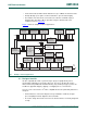
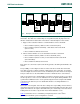
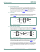
UM10204 NXP Semiconductors I2C-bus specification and user manual LCD DRIVER MICRO CONTROLLER A STATIC RAM OR EEPROM SDA SCL GATE ARRAY MICRO CONTROLLER B ADC mbc645 Fig 2. Example of an I2C-bus configuration using two microcontrollers This example highlights the master-slave and receiver-transmitter relationships found on the I2C-bus. Note that these relationships are not permanent, but only depend on the direction of data transfer at that time. The transfer of data would proceed as follows: 1.
UM10204 NXP Semiconductors I2C-bus specification and user manual Table 2. Applicability of I2C-bus protocol features M = mandatory; O = optional; n/a = not applicable.
UM10204 NXP Semiconductors I2C-bus specification and user manual 3.1.2 SDA and SCL logic levels Due to the variety of different technology devices (CMOS, NMOS, bipolar) that can be connected to the I2C-bus, the levels of the logical ‘0’ (LOW) and ‘1’ (HIGH) are not fixed and depend on the associated level of VDD. Input reference levels are set as 30 % and 70 % of VDD; VIL is 0.3VDD and VIH is 0.7VDD. See Figure 38, timing diagram. Some legacy device input levels were fixed at VIL = 1.5 V and VIH = 3.
UM10204 NXP Semiconductors I2C-bus specification and user manual Detection of START and STOP conditions by devices connected to the bus is easy if they incorporate the necessary interfacing hardware. However, microcontrollers with no such interface have to sample the SDA line at least twice per clock period to sense the transition. 3.1.5 Byte format Every byte put on the SDA line must be eight bits long. The number of bytes that can be transmitted per transfer is unrestricted.
UM10204 NXP Semiconductors I2C-bus specification and user manual 3.1.7 Clock synchronization Two masters can begin transmitting on a free bus at the same time and there must be a method for deciding which takes control of the bus and complete its transmission. This is done by clock synchronization and arbitration. In single master systems, clock synchronization and arbitration are not needed. Clock synchronization is performed using the wired-AND connection of I2C interfaces to the SCL line.
UM10204 NXP Semiconductors I2C-bus specification and user manual transmissions are identical. The first time a master tries to send a HIGH, but detects that the SDA level is LOW, the master knows that it has lost the arbitration and turns off its SDA output driver. The other master goes on to complete its transaction. No information is lost during the arbitration process.
UM10204 NXP Semiconductors I2C-bus specification and user manual 3.1.9 Clock stretching Clock stretching pauses a transaction by holding the SCL line LOW. The transaction cannot continue until the line is released HIGH again. Clock stretching is optional and in fact, most slave devices do not include an SCL driver so they are unable to stretch the clock.
UM10204 NXP Semiconductors I2C-bus specification and user manual Possible data transfer formats are: • Master-transmitter transmits to slave-receiver. The transfer direction is not changed (see Figure 11). The slave receiver acknowledges each byte. • Master reads slave immediately after first byte (see Figure 12). At the moment of the first acknowledge, the master-transmitter becomes a master-receiver and the slave-receiver becomes a slave-transmitter.
UM10204 NXP Semiconductors I2C-bus specification and user manual S SLAVE ADDRESS R/W A DATA A DATA A/A P data transferred (n bytes + acknowledge) '0' (write) from master to slave A = acknowledge (SDA LOW) from slave to master A = not acknowledge (SDA HIGH) S = START condition P = STOP condition mbc605 Fig 11.
UM10204 NXP Semiconductors I2C-bus specification and user manual All combinations of read/write formats previously described for 7-bit addressing are possible with 10-bit addressing. Two are detailed here: • Master-transmitter transmits to slave-receiver with a 10-bit slave address. The transfer direction is not changed (see Figure 14).
UM10204 NXP Semiconductors I2C-bus specification and user manual The START byte 0000 0001 (01h) can precede the 10-bit addressing in the same way as for 7-bit addressing (see Section 3.1.15). 3.1.12 Reserved addresses Two groups of eight addresses (0000 XXX and 1111 XXX) are reserved for the purposes shown in Table 3. Table 3. Reserved addresses X = don’t care; 1 = HIGH; 0 = LOW.
UM10204 NXP Semiconductors I2C-bus specification and user manual LSB 0 0 0 0 0 0 0 0 A X X X X X X X B A first byte (general call address) second byte mbc623 Fig 16. General call address format There are two cases to consider: • When the least significant bit B is a ‘zero’. • When the least significant bit B is a ‘one’. When bit B is a ‘zero’, the second byte has the following definition: • 0000 0110 (06h): Reset and write programmable part of slave address by hardware.
UM10204 NXP Semiconductors I2C-bus specification and user manual In some systems, an alternative could be that the hardware master transmitter is set in the slave-receiver mode after the system reset. In this way, a system configuring master can tell the hardware master-transmitter (which is now in slave-receiver mode) to which address data must be sent (see Figure 18). After this programming procedure, the hardware master remains in the master-transmitter mode. S SLAVE ADDR.
UM10204 NXP Semiconductors I2C-bus specification and user manual dummy acknowledge (HIGH) SDA 1 SCL 2 7 8 9 NACK S START byte 0000 0001 Sr 002aac997 Fig 19. START byte procedure After the START condition S has been transmitted by a master which requires bus access, the START byte (0000 0001) is transmitted. Another microcontroller can therefore sample the SDA line at a low sampling rate until one of the seven zeros in the START byte is detected.
UM10204 NXP Semiconductors I2C-bus specification and user manual manufacturer 0 part identification 0 0 0 0 0 0 0 0 0 0 0 0 0 0 0 0 0 0 0 0 0 0 revision 0 002aab942 Fig 20. Device ID field The Device ID is read-only, hard-wired in the device and can be accessed as follows: 1. START condition 2. The master sends the Reserved Device ID I2C-bus address followed by the R/W bit set to ‘0’ (write): ‘1111 1000’. 3.
UM10204 NXP Semiconductors I2C-bus specification and user manual Table 4.
UM10204 NXP Semiconductors I2C-bus specification and user manual 3.2 Ultra Fast-mode I2C-bus protocol The UFm I2C-bus is a 2-wire push-pull serial bus that operates from DC to 5 MHz transmitting data in one direction. It is most useful for speeds greater than 1 MHz to drive LED controllers and other devices that do not need feedback. The UFm I2C-bus protocol is based on the standard I2C-bus protocol that consists of a START, slave address, command bit, ninth clock, and a STOP bit.
UM10204 NXP Semiconductors I2C-bus specification and user manual This highlights the master/transmitter-slave/receiver relationship found on the UFm I2C-bus. Note that these relationships are permanent, as data transfer is only permitted in one direction.
UM10204 NXP Semiconductors I2C-bus specification and user manual 3.2.1 USDA and USCL signals Both USDA and USCL are unidirectional lines, with push-pull outputs. When the bus is free, both lines are pulled HIGH by the upper transistor of the output stage. Data on the I2C-bus can be transferred at rates of up to 5000 kbit/s in the Ultra Fast-mode. The number of interfaces connected to the bus is limited by the bus loading, reflections from cable ends, connectors, and stubs.
UM10204 NXP Semiconductors I2C-bus specification and user manual USDA USCL S P START condition STOP condition 002aaf145 Fig 24. Definition of START and STOP conditions for UFm I2C-bus START and STOP conditions are always generated by the master. The bus is considered to be busy after the START condition. The bus is considered to be free again a certain time after the STOP condition. This bus free situation is specified in Section 6.
UM10204 NXP Semiconductors I2C-bus specification and user manual 3.2.6 Acknowledge (ACK) and Not Acknowledge (NACK) Since the slaves are not able to respond the ninth clock cycle, the ACK and NACK are not required. However, the clock cycle is preserved in the UFm to be compatible with the I2C-bus protocol. The ACK and NACK are also referred to as the ninth clock cycle. The master generates all clock pulses, including the ninth clock pulse. The ninth data bit is always driven HIGH (‘1’).
UM10204 NXP Semiconductors I2C-bus specification and user manual S SLAVE ADDRESS W ‘0’ (write) from master to slave A DATA A DATA A P data transferred (n bytes + not acknowledge) A = not acknowledge (USDA HIGH) S = START condition P = STOP condition 002aag660 Fig 28. A master-transmitter addressing a slave receiver with a 7-bit address Notes: 1. Individual transaction or repeated START formats addressing multiple slaves in one transaction can be used.
UM10204 NXP Semiconductors I2C-bus specification and user manual Only the write format previously described for 7-bit addressing is possible with 10-bit addressing. Detailed here: • Master-transmitter transmits to slave-receiver with a 10-bit slave address. The transfer direction is not changed (see Figure 29).
UM10204 NXP Semiconductors I2C-bus specification and user manual 3.2.10 General call address The general call address is for addressing every device connected to the I2C-bus at the same time. However, if a device does not need any of the data supplied within the general call structure, it can ignore this address. If a device does require data from a general call address, it behaves as a slave-receiver. The master does not actually know how many devices are responsive to the general call.
UM10204 NXP Semiconductors I2C-bus specification and user manual In this case, data transfer can be preceded by a start procedure which is much longer than normal (see Figure 31). The start procedure consists of: • • • • A START condition (S) A START byte (0000 0001) A Not Acknowledge clock pulse (NACK) A repeated START condition (Sr) dummy acknowledge (HIGH) USDA 1 USCL 2 7 8 9 NACK S START byte 0000 0001 Sr 002aag663 Fig 31.
UM10204 NXP Semiconductors I2C-bus specification and user manual 4. Other uses of the I2C-bus communications protocol The I2C-bus is used as the communications protocol for several system architectures. These architectures have added command sets and application-specific extensions in addition to the base I2C specification. In general, simple I2C-bus devices such as I/O extenders could be used in any one of these architectures since the protocol and physical interfaces are the same. 4.
UM10204 NXP Semiconductors I2C-bus specification and user manual Logic levels are slightly different also: TTL for SMBus: LOW = 0.8 V and HIGH = 2.1 V, versus the 30 %/70 % VDD CMOS level for I2C. This is not a problem if VDD > 3.0 V. If the I2C device is below 3.0 V, then there could be a problem if the logic HIGH/LOW levels are not properly recognized. 4.2.2 Time-out feature SMBus has a time-out feature which resets devices if a communication takes too long.
UM10204 NXP Semiconductors I2C-bus specification and user manual 4.3 PMBus - Power Management Bus PMBus is a standard way to communicate between power converters and a system host over the SMBus to provide more intelligent control of the power converters. The PMBus specification defines a standard set of device commands so that devices from multiple sources function identically. PMBus devices use the SMBus Version 1.1 plus extensions for transport. For more information, refer to: www.pmbus.org/. 4.
UM10204 NXP Semiconductors I2C-bus specification and user manual 4.5 Advanced Telecom Computing Architecture (ATCA) Advanced Telecom Computing Architecture (ATCA) is a follow-on to Compact PCI (cPCI), providing a standardized form-factor with larger card area, larger pitch and larger power supply for use in advanced rack-mounted telecom hardware. It includes a fault-tolerant scheme for thermal management that uses I2C-bus communications between boards.
UM10204 NXP Semiconductors I2C-bus specification and user manual 5.1 Fast-mode Fast-mode devices can receive and transmit at up to 400 kbit/s. The minimum requirement is that they can synchronize with a 400 kbit/s transfer; they can then prolong the LOW period of the SCL signal to slow down the transfer. The protocol, format, logic levels and maximum capacitive load for the SDA and SCL lines are the same as the Standard-mode I2C-bus specification.
UM10204 NXP Semiconductors I2C-bus specification and user manual 5.3 Hs-mode High-speed mode (Hs-mode) devices offer a quantum leap in I2C-bus transfer speeds. Hs-mode devices can transfer information at bit rates of up to 3.4 Mbit/s, yet they remain fully downward compatible with Fast-mode Plus, Fast- or Standard-mode (F/S) devices for bidirectional communication in a mixed-speed bus system.
UM10204 NXP Semiconductors I2C-bus specification and user manual proceeded by an acknowledge bit, the rise time of the SCLH clock pulses in Hs-mode transfers is shortened by the internal current-source pull-up circuit MCS of the active master.
UM10204 NXP Semiconductors I2C-bus specification and user manual Arbitration and clock synchronization only take place during the transmission of the master code and not-acknowledge bit (A), after which one winning master remains active. The master code indicates to other devices that an Hs-mode transfer is to begin and the connected devices must meet the Hs-mode specification. As no device is allowed to acknowledge the master code, the master code is followed by a not-acknowledge (A).
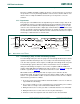
UM10204 NXP Semiconductors I2C-bus specification and user manual A 8-bit master code 0000 1xxx S t1 tH SDA high SCL high 1 2 to 5 6 7 8 9 F/S mode R/W 7-bit SLA Sr n + (8-bit data A + A/A) Sr P SDA high SCL high 1 2 to 5 6 7 8 9 1 2 to 5 6 7 8 9 If P then F/S mode HS mode If Sr (dotted lines) then HS mode tH tFS = Master current source pull-up msc618 = Resistor pull-up Fig 34. A complete Hs-mode transfer 5.3.
UM10204 NXP Semiconductors I2C-bus specification and user manual The non-active, or losing masters: 1. Adapt their SDAH and SCLH input filters according to the spike suppression requirement in Hs-mode. 2. Wait for a STOP condition to detect when the bus is free again. All slaves: 1. Adapt their SDAH and SCLH input filters according to the spike suppression requirement in Hs-mode. 2. Adapt the set-up and hold times according to the Hs-mode requirements.
UM10204 NXP Semiconductors I2C-bus specification and user manual VDD Rp Rp SDA SCL Rs Rs Rs Rs Rs Rs Rs (1) SDAH (2) SCLH SDAH (2) (2) SCLH SDAH (2) (4) (2) SCLH SDA Rs Rs SCL (2) SDA (2) SCL SDA (2) (2) SCL (2) (3) (4) Rs (1) (4) VDD VSS VSS Hs-mode SLAVE Hs-mode SLAVE VSS VSS Hs-mode MASTER/SLAVE VSS F/S-mode MASTER/SLAVE F/S-mode SLAVE msc613 (1) Bridge not used. SDA and SCL may have an alternative function. (2) To input filter.
UM10204 NXP Semiconductors I2C-bus specification and user manual opens to separate the two bus sections and allows Hs-mode devices to communicate with each other at 3.4 Mbit/s. Arbitration between Hs-mode devices and F/S-mode devices is only performed during the master code (0000 1XXX), and normally won by one Hs-mode master as no slave address has four leading zeros. Other masters can win the arbitration only if they send a reserved 8-bit code (0000 0XXX).
UM10204 NXP Semiconductors I2C-bus specification and user manual 5.3.6 Standard, Fast-mode and Fast-mode Plus transfer in a mixed-speed bus system The bridge shown in Figure 36 interconnects corresponding serial bus lines, forming one serial bus system. As no master code (0000 1XXX) is transmitted, the current-source pull-up circuits stay disabled and all output stages are open-drain.
UM10204 NXP Semiconductors I2C-bus specification and user manual 8-bit Master code 00001xxx S A t1 tH SDAH SCLH 1 2 to 5 6 7 8 9 1 2 to 5 6 7 8 9 SDA SCL F/S mode R/W 7-bit SLA Sr n × (8-bit DATA A + A/A) Sr P SDAH SCLH 1 2 to 5 6 7 8 9 1 2 to 5 6 7 8 9 P SDA t2 SCL If P then F/S mode Hs-mode If Sr (dotted lines) then Hs-mode tH tFS mcs611 = MCS current source pull-up = Rp resistor pull-up Fig 37.
UM10204 NXP Semiconductors I2C-bus specification and user manual 5.4 Ultra Fast-mode Ultra Fast-mode (UFm) devices offer an increase in I2C-bus transfer speeds. UFm devices can transfer information at bit rates of up to 5 Mbit/s. UFm devices offer push-pull drivers, eliminating the pull-up resistors, allowing higher transfer rates. The same serial bus protocol and data format is maintained as with the Sm, Fm, or Fm+ system. UFm bus devices are not compatible with bidirectional I2C-bus devices. 6.
xxxxxxxxxxxxxxxxxxxxx xxxxxxxxxxxxxxxxxxxxxxxxxx xxxxxxx x x x xxxxxxxxxxxxxxxxxxxxxxxxxxxxxx xxxxxxxxxxxxxxxxxxx xx xx xxxxx xxxxxxxxxxxxxxxxxxxxxxxxxxx xxxxxxxxxxxxxxxxxxx xxxxxx xxxxxxxxxxxxxxxxxxxxxxxxxxxxxxxxxxx xxxxxxxxxxxx x x xxxxxxxxxxxxxxxxxxxxx xxxxxxxxxxxxxxxxxxxxxxxxxxxxxx xxxxx xxxxxxxxxxxxxxxxxxxxxxxxxxxxxxxxxxxxxxxxxxxxxxxxxx xxxxxxxx xxxxxxxxxxxxxxxxxxxxxxxxx xxxxxxxxxxxxxxxxxxxx xxx NXP Semiconductors UM10204 User manual Table 9.
xxxxxxxxxxxxxxxxxxxxx xxxxxxxxxxxxxxxxxxxxxxxxxx xxxxxxx x x x xxxxxxxxxxxxxxxxxxxxxxxxxxxxxx xxxxxxxxxxxxxxxxxxx xx xx xxxxx xxxxxxxxxxxxxxxxxxxxxxxxxxx xxxxxxxxxxxxxxxxxxx xxxxxx xxxxxxxxxxxxxxxxxxxxxxxxxxxxxxxxxxx xxxxxxxxxxxx x x xxxxxxxxxxxxxxxxxxxxx xxxxxxxxxxxxxxxxxxxxxxxxxxxxxx xxxxx xxxxxxxxxxxxxxxxxxxxxxxxxxxxxxxxxxxxxxxxxxxxxxxxxx xxxxxxxx xxxxxxxxxxxxxxxxxxxxxxxxx xxxxxxxxxxxxxxxxxxxx xxx Characteristics of the SDA and SCL bus lines for Standard, Fast, and Fast-mode Plus I2C-bus devices[1] Symb
xxxxxxxxxxxxxxxxxxxxx xxxxxxxxxxxxxxxxxxxxxxxxxx xxxxxxx x x x xxxxxxxxxxxxxxxxxxxxxxxxxxxxxx xxxxxxxxxxxxxxxxxxx xx xx xxxxx xxxxxxxxxxxxxxxxxxxxxxxxxxx xxxxxxxxxxxxxxxxxxx xxxxxx xxxxxxxxxxxxxxxxxxxxxxxxxxxxxxxxxxx xxxxxxxxxxxx x x xxxxxxxxxxxxxxxxxxxxx xxxxxxxxxxxxxxxxxxxxxxxxxxxxxx xxxxx xxxxxxxxxxxxxxxxxxxxxxxxxxxxxxxxxxxxxxxxxxxxxxxxxx xxxxxxxx xxxxxxxxxxxxxxxxxxxxxxxxx xxxxxxxxxxxxxxxxxxxx xxx A Fast-mode I2C-bus device can be used in a Standard-mode I2C-bus system, but the requirement tSU;DAT 250 ns
UM10204 NXP Semiconductors I2C-bus specification and user manual tf SDA tr tSU;DAT 70 % 30 % 70 % 30 % cont. tHD;DAT tf tVD;DAT tHIGH tr 70 % 30 % SCL 70 % 30 % 70 % 30 % tHD;STA 70 % 30 % cont. tLOW 9th clock 1 / fSCL S 1st clock cycle tBUF SDA tSU;STA tHD;STA tVD;ACK tSP tSU;STO 70 % 30 % SCL Sr P 9th clock S 002aac938 VIL = 0.3VDD VIH = 0.7VDD Fig 38. Definition of timing for F/S-mode devices on the I2C-bus 6.
UM10204 NXP Semiconductors I2C-bus specification and user manual capacitive bus loads between 100 pF and 400 pF, the timing parameters must be interpolated linearly. Rise and fall times are in accordance with the maximum propagation time of the transmission lines SDAH and SCLH to prevent reflections of the open ends. Table 11. Characteristics of the SDAH, SCLH, SDA and SCL I/O stages for Hs-mode I2C-bus devices Symbol Parameter Conditions Hs-mode Unit Min Max 0.
UM10204 NXP Semiconductors I2C-bus specification and user manual Table 12. Characteristics of the SDAH, SCLH, SDA and SCL bus lines for Hs-mode I2C-bus devices[1] Symbol Parameter fSCLH SCLH clock frequency tSU;STA Conditions Cb = 400 pF[2] Cb = 100 pF (max) Unit Min Max Min Max 0 3.4 0 1.
UM10204 NXP Semiconductors I2C-bus specification and user manual Sr Sr trDA tfDA P 0.7 × VDD 0.3 × VDD SDAH tHD;DAT tSU;STA tSU;STO tSU;DAT tHD;STA 0.7 × VDD 0.3 × VDD SCLH trCL1 tfCL (1) trCL1 trCL tHIGH tLOW tLOW (1) tHIGH 002aag825 = MCS current source pull-up = Rp resistor pull-up (1) First rising edge of the SCLH signal after Sr and after each acknowledge bit. Fig 39. Definition of timing for Hs-mode devices on the I2C-bus 6.
UM10204 NXP Semiconductors I2C-bus specification and user manual Table 14.
UM10204 NXP Semiconductors I2C-bus specification and user manual 7. Electrical connections of I2C-bus devices to the bus lines 7.1 Pull-up resistor sizing The bus capacitance is the total capacitance of wire, connections and pins. This capacitance limits the maximum value of Rp due to the specified rise time. Figure 41 shows Rp(max) as a function of bus capacitance. Consider the VDD related input threshold of VIH = 0.7VDD and VIL = 0.3VDD for the purposes of RC time constant calculation.
UM10204 NXP Semiconductors I2C-bus specification and user manual The designer now has the minimum and maximum value of Rp that is required to meet the timing specification. Portable designs with sensitivity to supply current consumption can use a value toward the higher end of the range in order to limit IDD. 7.2 Operating above the maximum allowable bus capacitance Bus capacitance limit is specified to limit rise time reductions and allow operating at the rated frequency.
UM10204 NXP Semiconductors I2C-bus specification and user manual capacitance. Keep in mind that adding a buffer always adds delays — a buffer delay plus an additional transition time to each edge, which reduces the maximum operating frequency and may also introduce special VIL and VOL considerations.
UM10204 NXP Semiconductors I2C-bus specification and user manual The switched pull-up circuit in Figure 44 is for a supply voltage of VDD = 5 V ± 10 % and a maximum capacitive load of 400 pF. Since it is controlled by the bus levels, it needs no additional switching control signals. During the rising/falling edges, the bilateral switch in the HCT4066 switches pull-up resistor Rp2 on/off at bus levels between 0.8 V and 2.0 V.
UM10204 NXP Semiconductors I2C-bus specification and user manual mbc629 10 Rp (kΩ) 5V VDD = 2.5 V 8 6 15 V 4 10 V 2 0 0 400 800 1200 1600 maximum value Rs (Ω) Fig 46. Maximum value of Rs as a function of the value of Rp with supply voltage as a parameter 7.4 Input leakage The maximum HIGH level input current of each input/output connection has a specified maximum value of 10 μA. Due to the required noise margin of 0.2VDD for the HIGH level, this input current limits the maximum value of Rp.
UM10204 NXP Semiconductors I2C-bus specification and user manual 7.5 Wiring pattern of the bus lines In general, the wiring must be chosen so that crosstalk and interference to/from the bus lines is minimized. The bus lines are most susceptible to crosstalk and interference at the HIGH level because of the relatively high impedance of the pull-up devices.
UM10204 NXP Semiconductors I2C-bus specification and user manual 8. Abbreviations Table 15.
UM10204 NXP Semiconductors I2C-bus specification and user manual 9. Legal information 9.1 Definitions Draft — The document is a draft version only. The content is still under internal review and subject to formal approval, which may result in modifications or additions. NXP Semiconductors does not give any representations or warranties as to the accuracy or completeness of information included herein and shall have no liability for the consequences of use of such information. 9.
UM10204 NXP Semiconductors I2C-bus specification and user manual 10. Contents 1 2 2.1 2.2 2.3 3 3.1 3.1.1 3.1.2 3.1.3 3.1.4 3.1.5 3.1.6 3.1.7 3.1.8 3.1.9 3.1.10 3.1.11 3.1.12 3.1.13 3.1.14 3.1.15 3.1.16 3.1.17 3.2 3.2.1 3.2.2 3.2.3 3.2.4 3.2.5 3.2.6 3.2.7 3.2.8 3.2.9 3.2.10 3.2.11 3.2.12 3.2.13 3.2.14 4 4.1 4.2 4.2.1 Introduction . . . . . . . . . . . . . . . . . . . . . . . . . . . . 3 I2C-bus features . . . . . . . . . . . . . . . . . . . . . . . . . 3 Designer benefits . . . . . . . . . . . . . . . .
UM10204 NXP Semiconductors I2C-bus specification and user manual 9 9.1 9.2 9.3 10 Legal information. . . . . . . . . . . . . . . . . . . . . . . Definitions . . . . . . . . . . . . . . . . . . . . . . . . . . . . Disclaimers . . . . . . . . . . . . . . . . . . . . . . . . . . . Trademarks. . . . . . . . . . . . . . . . . . . . . . . . . . . Contents . . . . . . . . . . . . . . . . . . . . . . . . . . . . . .