
Data Sheet

UM10204 All information provided in this document is subject to legal disclaimers. © NXP Semiconductors N.V. 2014. All rights reserved.
User manual Rev. 6 — 4 April 2014 24 of 64
NXP Semiconductors
UM10204
I
2
C-bus specification and user manual
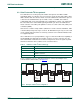
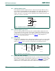
This highlights the master/transmitter-slave/receiver relationship found on the UFm
I
2
C-bus. Note that these relationships are permanent, as data transfer is only permitted in
one direction. The transfer of data would proceed as follows:
Suppose that the master ASIC wants to send information to the LED controller 2:
• ASIC A (master-transmitter), addresses LED controller 2 (slave-receiver) by sending
the address on the USDA and generating the clock on USCL.
• ASIC A (master-transmitter), sends data to LED controller 2 (slave-receiver) on the
USDA and generates the clock on USCL.
• ASIC A terminates the transfer.
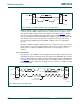
The possibility of connecting more than one UFm master to the UFm I
2
C-bus is not
allowed due to bus contention on the push-pull outputs. If an additional master is required
in the system, it must be fully isolated from the other master (that is, with a true ‘one hot’
MUX) as only one master is allowed on the bus at a time.
Generation of clock signals on the UFm I
2
C-bus is always the responsibility of the master
device, that is, the master generates the clock signals when transferring data on the bus.
Bus clock signals from a master cannot be altered by a slave device with clock stretching
and the process of arbitration and clock synchronization does not exist within the UFm
I
2
C-bus.
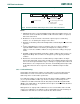
Table 6
summarizes the use of mandatory and optional portions of the UFm I
2
C-bus
specification.
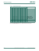
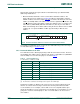
Table 6. Applicability of I
2
C-bus features to UFm
M = mandatory; O = optional; n/p = not possible
Feature Configuration
Single master
START condition M
STOP condition M
Acknowledge n/p
Synchronization n/p
Arbitration n/p
Clock stretching n/p
7-bit slave address M
10-bit slave address O
General Call address O
Software Reset O
START byte O
Device ID n/p