
Data Sheet

UM10204 All information provided in this document is subject to legal disclaimers. © NXP Semiconductors N.V. 2014. All rights reserved.
User manual Rev. 6 — 4 April 2014 25 of 64
NXP Semiconductors
UM10204
I
2
C-bus specification and user manual
3.2.1 USDA and USCL signals
Both USDA and USCL are unidirectional lines, with push-pull outputs. When the bus is
free, both lines are pulled HIGH by the upper transistor of the output stage. Data on the
I
2
C-bus can be transferred at rates of up to 5000 kbit/s in the Ultra Fast-mode. The
number of interfaces connected to the bus is limited by the bus loading, reflections from
cable ends, connectors, and stubs.
3.2.2 USDA and USCL logic levels
Due to the variety of different technology devices (CMOS, NMOS, bipolar) that can be
connected to the I
2
C-bus, the levels of the logical ‘0’ (LOW) and ‘1’ (HIGH) are not fixed
and depend on the associated level of V
DD
. Input reference levels are set as 30 % and
70 % of V
DD
; V
IL
is 0.3V
DD
and V
IH
is 0.7V
DD
. See Figure 40, timing diagram. See
Section 6
for electrical specifications.
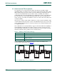
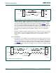
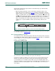
3.2.3 Data validity
The data on the USDA line must be stable during the HIGH period of the clock. The HIGH
or LOW state of the data line can only change when the clock signal on the USCL line is
LOW (see Figure 23
). One clock pulse is generated for each data bit transferred.
3.2.4 START and STOP conditions
Both data and clock lines remain HIGH when the bus is not busy. All transactions begin
with a START (S) and can be terminated by a STOP (P) (see Figure 24
). A HIGH to LOW
transition on the USDA line while USCL is HIGH defines a START condition. A LOW to
HIGH transition on the USDA line while USCL is HIGH defines a STOP condition.
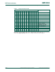
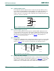
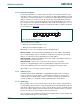
Fig 22. Simplified schematic of USCL, USDA outputs
002aag655
V
DD(IO)
V
SS
USCL or
USDA pin
Fig 23. Bit transfer on the UFm I
2
C-bus
002aaf113
data line
stable;
data valid
change
of data
allowed
USDA
USCL