
Data Sheet

UM10204 All information provided in this document is subject to legal disclaimers. © NXP Semiconductors N.V. 2014. All rights reserved.
User manual Rev. 6 — 4 April 2014 53 of 64
NXP Semiconductors
UM10204
I
2
C-bus specification and user manual
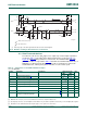
6.3 Ultra Fast-mode devices
The I/O levels, I/O current, spike suppression, output slope control and pin capacitance
are given in Table 13
. The UFm I
2
C-bus timing characteristics are given in Table 14.
Figure 40
shows the timing definitions for the I
2
C-bus. The minimum HIGH and LOW
periods of the SCL clock specified in Table 14
determine the maximum bit transfer rates of
5000 kbit/s for Ultra Fast-mode. Devices must be able to follow transfers at their own
maximum bit rates, either by being able to transmit or receive at that speed.
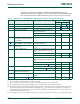
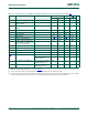
[1] Refer to component data sheets for actual switching points.
[2] Maximum V
IH
= V
DD(max)
+ 0.5 V or 5.5 V, whichever is lower. See component data sheets.
[3] Special purpose devices such as multiplexers and switches may exceed this capacitance because they connect multiple paths together.
[4] Input filters on the USDA and USCL slave inputs suppress noise spikes of less than 10 ns.
(1) First rising edge of the SCLH signal after Sr and after each acknowledge bit.
Fig 39. Definition of timing for Hs-mode devices on the I
2
C-bus
002aag825
SDAH
SrSr P
SCLH
= MCS current source pull-up
= Rp resistor pull-up
t
fDA
t
rDA
t
HD;STA
t
SU;DAT
t
rCL
t
LOW
t
HIGH
t
HD;DAT
t
LOW
t
HIGH
t
rCL1
t
fCL
t
SU;STO
t
rCL1
(1)
(1)
t
SU;STA
0.7 × V
DD
0.3 × V
DD
0.7 × V
DD
0.3 × V
DD
Table 13. Characteristics of the USDA and USCL I/O stages
n/a = not applicable.
Symbol Parameter Conditions Ultra Fast-mode Unit
Min Max
V
IL
LOW-level input voltage
[1]
−0.5 +0.3V
DD
V
V
IH
HIGH-level input voltage
[1]
0.7V
DD
[1]
-
[2]
V
V
hys
hysteresis of Schmitt trigger inputs 0.05V
DD
-V
V
OL
LOW-level output voltage at 4 mA sink current; V
DD
>2V 0 0.4 V
V
OH
HIGH-level output voltage at 4 mA source current; V
DD
>2V V
DD
− 0.4 - V
I
L
leakage current V
DD
=3.6V −1+1μA
V
DD
=5.5V −10 +10 μA
C
i
input capacitance
[3]
-10pF
t
SP
pulse width of spikes that must
be suppressed by the input filter
[4]
-10ns