
Data Sheet

UM10204 All information provided in this document is subject to legal disclaimers. © NXP Semiconductors N.V. 2014. All rights reserved.
User manual Rev. 6 — 4 April 2014 57 of 64
NXP Semiconductors
UM10204
I
2
C-bus specification and user manual
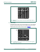
capacitance. Keep in mind that adding a buffer always adds delays — a buffer delay plus
an additional transition time to each edge, which reduces the maximum operating
frequency and may also introduce special V
IL
and V
OL
considerations.
Refer to application notes AN255, I
2
C / SMBus Repeaters, Hubs and Expanders and
AN262, PCA954x Family of I
2
C / SMBus Multiplexers and Switches for more details on
this subject and the devices available from NXP Semiconductors.
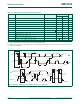
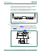
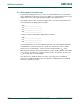
7.2.4 Switched pull-up circuit
The supply voltage (V
DD
) and the maximum output LOW level determine the minimum
value of pull-up resistor R
p
(see Section 7.1). For example, with a supply voltage of
V
DD
=5V± 10 % and V
OL(max)
= 0.4 V at 3 mA, R
p(min)
=(5.5− 0.4) / 0.003 = 1.7 kΩ. As
shown in Figure 42
, this value of R
p
limits the maximum bus capacitance to about 200 pF
to meet the maximum t
r
requirement of 300 ns. If the bus has a higher capacitance than
this, a switched pull-up circuit (as shown in Figure 44
) can be used.
Remark: Some buffers allow V
DD1
and V
DD2
to be different levels.
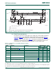
Fig 43. Using a buffer to divide bus capacitance
BUFFER
002aac882
V
DD1
SDA
SCL
slaves and masters
400 pF
slaves and masters
400 pF
V
DD2
Fig 44. Switched pull-up circuit
mbc620
1.3 kΩ
V
CC
V
SS
I/O
C
b
V
DD
SDA or SCL
bus line
NP
1/4 HCT4066
nZ GND
nE
nY
5V 10 %
R
p2
1.7 kΩ
R
p1
100 Ω
R
s
N
I/O
100 Ω
R
s
N
400 pF
max.
FAST - MODE I C BUS DEVICES
2