
Data Sheet

UM10204 All information provided in this document is subject to legal disclaimers. © NXP Semiconductors N.V. 2014. All rights reserved.
User manual Rev. 6 — 4 April 2014 8 of 64
NXP Semiconductors
UM10204
I
2
C-bus specification and user manual
[1] Also refers to a master acting as a slave.
[2] Clock stretching is a feature of some slaves. If no slaves in a system can stretch the clock (hold SCL LOW),
the master need not be designed to handle this procedure.
[3] ‘Bit banging’ (software emulation) multi-master systems should consider a START byte. See
Section 3.1.15
.
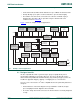
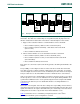
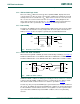
3.1.1 SDA and SCL signals
Both SDA and SCL are bidirectional lines, connected to a positive supply voltage via a
current-source or pull-up resistor (see Figure 3
). When the bus is free, both lines are
HIGH. The output stages of devices connected to the bus must have an open-drain or
open-collector to perform the wired-AND function. Data on the I
2
C-bus can be transferred
at rates of up to 100 kbit/s in the Standard-mode, up to 400 kbit/s in the Fast-mode, up to
1 Mbit/s in Fast-mode Plus, or up to 3.4 Mbit/s in the High-speed mode. The bus
capacitance limits the number of interfaces connected to the bus.
For a single master application, the master’s SCL output can be a push-pull driver design
if there are no devices on the bus which would stretch the clock.
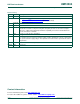
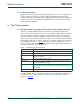
Table 2. Applicability of I
2
C-bus protocol features
M = mandatory; O = optional; n/a = not applicable.
Feature Configuration
Single master Multi-master Slave
[1]
START condition M M M
STOP condition M M M
Acknowledge M M M
Synchronization n/a M n/a
Arbitration n/a M n/a
Clock stretching O
[2]
O
[2]
O
7-bit slave address M M M
10-bit slave address O O O
General Call address O O O
Software Reset O O O
START byte n/a O
[3]
n/a
Device ID n/a n/a O
V
DD2
, V
DD3
are device-dependent (for example, 12 V).
Fig 3. Devices with various supply voltages sharing the same bus
CMOS CMOS NMOS BIPOLAR
002aac860
V
DD1
=
5 V ± 10 %
R
p
R
p
SDA
SCL
V
DD2
V
DD3