PRODUCT SPECIFICATION DECT application module Model no.: KT4586 POLYCOM ED 2.0 DATE Model no.
PRODUCT SPECIFICATION 1. Preface ....................................................................................................................................... 3 2. Features ..................................................................................................................................... 3 3. Circuit description ..................................................................................................................... 4 4. Pin configuration .....................
PRODUCT SPECIFICATION 1. Preface The KT4586, DECT application module is used to transfer messaging, data, and voice signals by use of the radio frequency spectrum according to the DECT standard. KT4586 is a fully approved module that complies with the following standards and certifications: EN 301 406 V2.1.1:2009-07 (DECT radio) EN 300 175-1 to 8 (DECT CI) EN 301 489-1 V1.8.1:2008-04, EN 301 489-6 V1.3.1:2008-08 (EMC) IEC 60950-1:2005 (ed. 2.
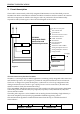
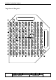
PRODUCT SPECIFICATION 3. Circuit description The module consists mainly of the fully integrated CMOS transceiver and baseband processor SC14441 from SiTel semiconductor intended for DECT 6.0 handsets and base stations. RF switches and other components are added to the design in order to perform the desired functionality required for DECT/GAP. Figure 1 shows the block diagram of the module. Ant.
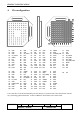
PRODUCT SPECIFICATION 4.
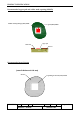
PRODUCT SPECIFICATION Top view of the pin’s POLYCOM ED 2.0 DATE Model no.
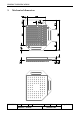
PRODUCT SPECIFICATION 5. Mechanical dimension POLYCOM ED 2.0 DATE Model no.
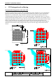
PRODUCT SPECIFICATION 6. PCB integration & soldering Recommended integration on the main PCB In order to ensure proper coverage and to avoid detuning of the antennas, it is very important to place the module in a free prober way on the main board and in relation to other surrounding materials. As a “thumb rule”, keep a distance of at least 10 mm from the antenna element to conducting objects and at least 5 mm to non-conducting objects - depending of the size.
PRODUCT SPECIFICATION Recommended copper pad and solder mask opening (NSMD) So ld er ma sk op eni ng Solder mask opening 1.8 0x1 .8 m 0m 1.0 x 0 .0 d1 . pa 0m 1,00x1,00mmm CuCu. pad 0,80x0,80mm Copper pads Solder Mask Substrate Recommended stencil design (stencil thickness 0.122 mm) Stencil POLYCOM ED 2.0 Opening stencil Opening in in stencil 1.401,12x1,12mm x 1,40mm DATE Model no.
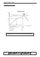
PRODUCT SPECIFICATION Recommended re-flow profile Reflow profile – leadfree Sn96.5-Ag3.0-Cu0.5 Temp. C° t3 t4 250° T3 220°C Meltingpoint 217°C 200° T2 190°C T1 150°C 150° 100° 50° t1 t2 0° Time t1: Max. Change in temperature t2: Time in preheat (150°C < temp. < 190°C) t3: Time in reflow zone (temp. > 220°C) t4: Peak temperature 3°C/sec. 60 - 120 sec. 30 - 60 sec.
PRODUCT SPECIFICATION 7. FCC compliance statement This device complies with Part 15 of the FCC Rules Operation is subject to the following two conditions: (1) this device may not cause interference, and (2) this device must accept any interference, including interference that may cause undesired operation of the device. Information to User: This equipment has been tested and found to comply with the limits for a Class B digital device, pursuant to Part 15 of the FCC Rules.
PRODUCT SPECIFICATION 8. Safety compliance statement 1) The specific external power supply for the DECT application module KT4585A has to fulfil the requirements according to clause 2.5 (Limited power source) of this standard EN 609501:2006. 2) Interconnection circuits shall be selected to provide continued conformance to the requirements of clause 2.2 for SELV (Safety Extra Low Voltage) circuits according to EN 60950-1:2006 after making connections. 3) Interface type not subjected to over voltages (i.e.