
User's Manual

SPA9323-30C Installation & Service Manual
© Copyright Powerwave Technologies, Inc., October 2004. All rights reserved
044-05178 Rev.A 4-1 October 2004
Section 4 Principles of Operation
4-1 Introduction
This section contains a functional description of the single-carrier SPA9323-30C amplifier.
4-2 RF Input Signal
The maximum input power should not exceed the levels to produce the maximum rated RF out-
put power in table 1-1. This level is approximately –3.2 dBm, but should be set through the base-
transceiver station’s software interface. See the BTS manual for detailed instructions.
4-3 RF Output Load
The load impedance should be as good as possible (1.5:1 or better) in the working band for good
power transfer to the load.
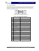
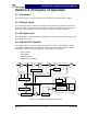
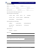
4-4 SPA9323-30C Amplifier
The amplifier, figure 4-1, has an average output power of 30 watts, and is designed to support
transmission in GMSK and EDGE modulation. With an input signal of approximately –3.2 dBm,
the amplifier operates at its rated output power. The amplifier is comprised of:
Driver Amplifier
Main Amplifier
Multifunction Board
DC/DC Converter Module
Multifunction
Main Amp
Temp Sense
Det
Driver
DAC
MCU
RS-485 Intfc
20-pin SCSI
3
PWR Conn
Red/
Grn
Input Filter/
Protection
Current Sense
DC/DC
-48/+27
5 V Reg.
Power Supply
+27
03-0217B-A
Figure 4-1 SPA9323-30C Amplifier Block Diagram