REVISIONS REVISION 1.0 DESCRIPTION APPROVED Preliminary Luis Vargas DATE 8/13/2010 GENERAL RELEASE DOCUMENT CONSULT FACTORY FOR CURRENT REVISION SPECIFICATION CONTROL DRAWING UNLESS OTHERWISE SPECIFIED, DIMENSIONS ARE IN INCHES. TOLERANCES: 3 PLACE DECIMAL = .005 2 PLACE DECIMAL = .02 1 PLACE DECIMAL = .1 FRACTIONS = ± 1/16 ANGLES = 2 DEGREES PREPARED BY: DATE Luis Vargas 8/13/10 CHECKED BY: DATE QUALITY RELEASED BY: APPROVED BY: DOCUMENT CONTROL ENGINEERING Q-TECH CORPORATION 10150 W.
1.0 SCOPE This specification establishes the detail requirements for low profile hybrid, hermetically sealed, HCMOS output Voltage Control Crystal Oscillators (VCXO) for use in space flight missions. 2.0 APPLICABLE DOCUMENTS The following documents of the latest issue form a part of this drawing to the extent specified herein. 2.
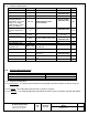
.1.1 Electrical Characteristics PARAMETER Frequency Nom. Supply voltage, Nom. Input Current, max. Overall Frequency stability (including Operating Temperature, ±5% Load Change, ±5% Supply Voltage change, 10 year aging, and radiation) Voltage Control Range For Frequency Adjustment Min. Control Voltage at which fo will occur at 25°C Frequency Pulling range, Min Linearity, max. Input impedance, min. Modulation freq. bandwidth, min. Output SYMBOL fo Vs Is Δf/fc (Ta) CONDITIONS VALUE 2.
3.2.2 Environmental Conditions Sine Vibration Random Vibration Shock Acceleration Altitude Radiation Electrostatic Discharge Sensitivity 3.
3.3.1 All piece parts shall be derived from lots that meet the element evaluation requirements of MIL-PRF38534, Class K with the following exceptions: Active elements a) Visual inspection of silicon on sapphire microcircuits. Semicircular crack(s) or multiple adjacent cracks, not in the active area, starting and terminating at the edge of the die are acceptable.
3.6.2. Technical Data Package. When required by the purchase order, the following design documentation and information is deliverable 30 days prior to the start of production. The Technical Data Package shall consist of the following: a) Assembly drawing(s). b) All electrical schematics and drawings not considered proprietary. c) The assembly and screening travelers to be used on-line to manufacture the devices supplied to this specification. d) Parts and materials list. 3.
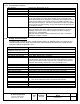
▀ PART NUMBER GENERATION SERIES QTV70: 24 Pin Double Dip Output Type, Supply Voltage, Voltage Control 1: HCMOS…5.0V Vc=0.5..4.5 2: HCMOS.,,3.3V Vc=0...3.3V TEMPERATURE RANGE (°C)/ Max. Overall Stability/ Min. APR and SYMMETRY FREQUENCY (MHz) Level A:40%…60% N: 0.....+50°C ±25 ppm ±50 ppm E: Eng. Model 2.000…90.000 (See note 1) T:(See note 2) P: 0.....+70°C ±35 ppm ±70 ppm M: Flight Model Q: 20…+70°C ±40 ppm ±80 ppm R: 40…+85°C ±45 ppm ±90 ppm U: -55.
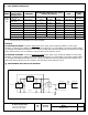
FIGURE 1 INTERFACE CONTROL DRAWING 24 Pin Double Dip Q-TECH USA PART NUMBER FREQUENCY D/C S/N ESD SYMBOL FOR PIN No. 1 .300 MAX. PIN NO. DESIGNATION 1 2 - 11 12 13 14 - 23 24 Voltage Control NC Ground/Case RF Output NC Supply Voltage 24X .200 MIN. 24X Ø .018 ± .002 22X .100 NON-ACCUMULATIVE 1.280 MAX. NOTES: • Dimensions are in inches. • Lead numbers are for reference only and are not marked on the unit. • A triangle symbol is marked on the corner of the package to indicate Pin 1.