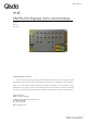
H18T Datasheet Datasheet H18T HSDPA PCI Express mini card module Datasheet Rev. 0.6 2010/04/06 Copyright Qisda Corporation This document contains proprietary technical information which is the property of Qisda Corporation and is issued in strict confidential and shall not be disclosed to others parties in whole or in parts without written permission of Qisda Corporation. The documents contain information on a product, which is under development and is issued for customer evaluation purposes only.
HISTORY Version Date Notes VER: 0.1 2009-NOV-05 PRELIMINARY VERSION VER:0.2 2009-DEC-24 UPDATED THICKNESS INFORMATION VER:0.3 2010-JAN-29 UPDATED PRODUCT PICTURE IN COVER PAGE VER:0.4 2010-MAR-12 REMOVE “E-DCH” SPECIFICATION DUE TO NO SUPPORT HSUPA VER:0.5 2010-MAR-19 UPDATED THE PEAK POWER CONDUMPTION PARAMETRIC VER:0.
1. INTRODUCTION..................................................................................................... 4 1.1 Description ...................................................................................................4 1.2 Application Device....................................................................................4 2. FEATURES ............................................................................................................... 5 2.1 General Characteristics ..............
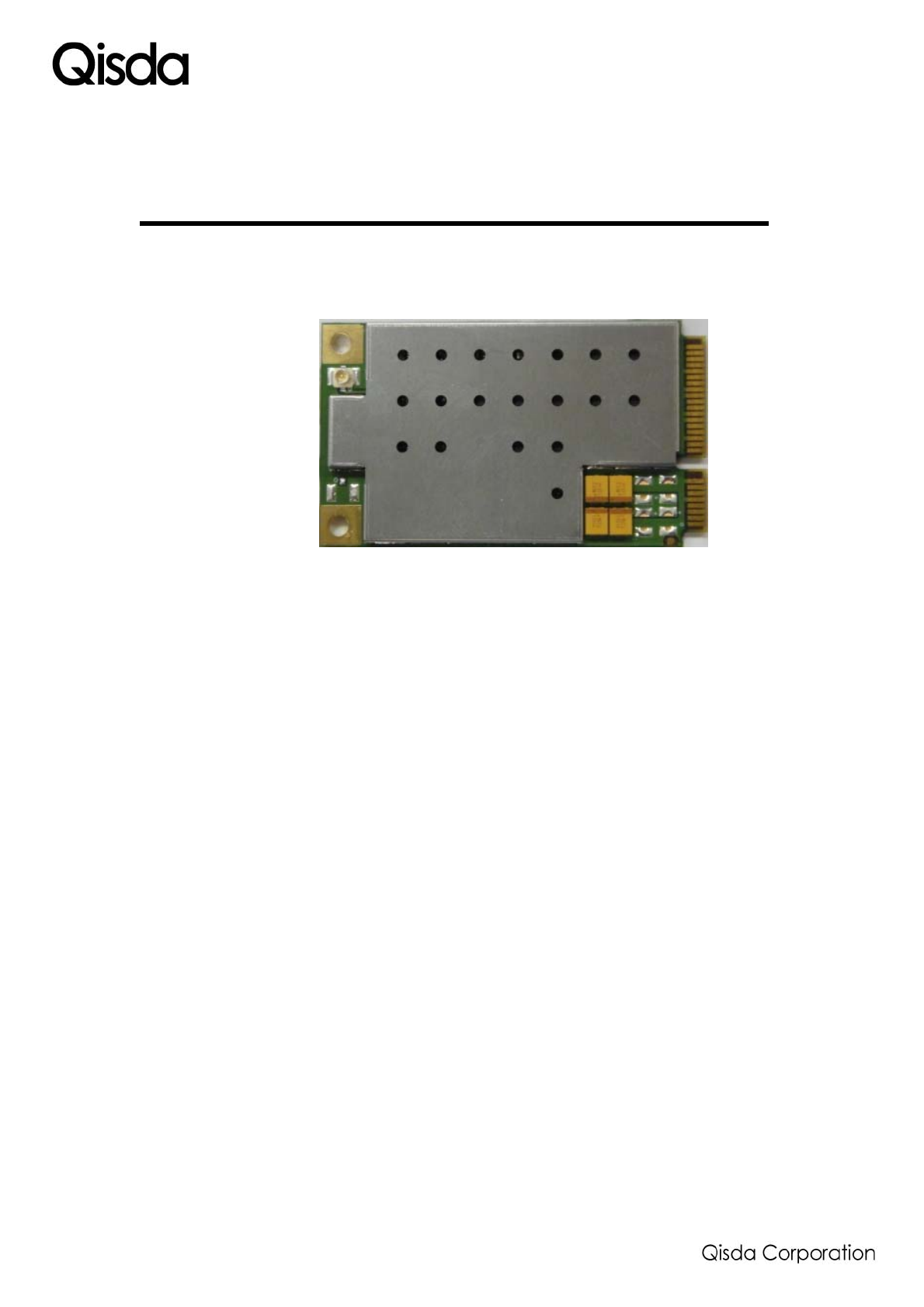
1. INTRODUCTION 1.1 Description Overview This document describes all the functions, features, and interfaces of the HSDPA PCI Express Mini Card Module – H18T from Qisda. Qisda H18T HSDPA module supports tri-band WCDMA/HSDPA and quad-band GSM/GPRS/EDGE network connection capability. Qisda H18T HSDPA card can provides high speed data connection, the data speed of downlink and uplink path is up to 3.6Mbps and 384Kbps respectively.
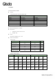
2. FEATURES 2.1 General Characteristics Bands: z Tri Band WCDMA and Quad Band GSM Band TX RX GSM850 824~849 MHz 869~894MHz EGSM900 880~915 MHz 925~960MHz DCS1800 1710~1785MHz 1805~1880MHz PCS1900 1850~1910MHz 1930~1990MHz WCDMA850 824~849 MHz 869~894MHz WCDMA1900 1850~1910MHz 1930~1990MHz WCDMA2100 1920~1980MHz 2110~2170MHz z Support SIM Interface: 1.8V/3V z Form factor z i. Dimension: 50.95 x 30 x 3.6 mm ii. Weight: 10g Power Operation Voltage: 3.3V ~ 3.
Sleeping Mode: z Typ (Average) Max (Average) Unit GSM / MFRM=2 5 6 mA GSM / MFRM =9 3 4.5 mA DCS / MFRM =2 5 6 mA DCS / MFRM =9 3.4 5 mA PCS / MFRM =2 5 6 mA PCS / Page frame=9 3.1 4.5 mA WCDMA / DRX=6 (0.64 S) 5.7 6.5 mA WCDMA / DRX=9 (5.12 S) 3.2 4.5 mA Shutdown current 10 50 uA Hardware Interface: 52 Pins PCI Express Mini Card connector interface 1 RF Antenna Coaxial Connectors z Software Interface: USB driver HSPA Modem software tool 2.
15/7≦βo/βd≦15/0 (HS-DPCCH) 22 dBm +3/-3dBm Parametric Performance Tests carried out at -20ºC, 25ºC and 60ºC for voltage 3.3V and 3.6V. The Measured Peak Phase, RMS Phase, frequency error, power level, and static sensitivity meets ETSI TS 151 010-1 chapter 13.1 for GSM and TS 34.121 chapter 5.13.1 for WCDMA, chapter 5.13.
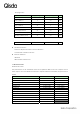
Channel Spacing 200 KHz Number of Channels 124 Carriers x 8 (TDMA) Modulation GMSK / 8-PSK Duplex Spacing 45 MHz Frequency Stability +/- 0.
Frequency Stability +/- 0.1 ppm (Uplink TX) Power Output 24 dBm +1/-3dBm - less than -50dBm Output Impedance 50 Ohm Spurious Emission -60dBm(869-894MHz;1930-1990MHz;2110-2155MHz) WCDMA_BC 5 (850 MHz) Frequency Range TX 824-849 MHz; RX 869-894 MHz Channel Raster 200KHz Number of Channels 299 Carriers x 8 (TDMA) Modulation QPSK Duplex Spacing 45 MHz Frequency Stability +/- 0.
3. HARDWARE DESCRIPTION 3.1 System Interface The I/O connectors of H18T module are PCI EXPRESS MINI CARD and two RF antenna connectors. Table 3-1 summarizes the signals and power lines that are supported by the PCI Express Mini Card System Interface. Table 3-2 shows the antenna interface. Table 3-1 System Interface Signal Group Pin counts. Description Power 5 3.3V power source GND 13 Return current path USB 2 USB serial data interface compliant to the USB 2.
3.
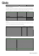
3.3 Pin Assignment and Description Pin Signal name Direction Description 1 NC Not connect 2 +3.3Vaux 3 NC 4 GND 5 NC No connect 6 NC No connect 7 NC No connect 8 UIM_PWR Output Power source for the USIM 9 GND Power Return current path 10 UIM_DATA 11 NC 12 UIM_CLK 13 NC 14 UIM_RESET Output USIM reset signal 15 GND Power Return current path 16 NC No connect 17 NC No connect 18 GND 19 NC Power 3.
32 NC No connect 33 NC No connect 34 GND Power Return current path 35 GND Power Return current path 36 USB_D- 37 GND 38 USB_D+ 39 +3.3Vaux Power 3.3V power source 40 GND Power Return current path 41 +3.3Vaux Power 3.3V power source 42 LED_WWAN# Output 43 GND Power 44 NC No connect 45 NC No connect 46 NC No connect 47 NC No connect 48 NC No connect 49 NC No connect 50 GND 51 NC 52 +3.
3.
System connector The Qisda H18T PCIE Express interface compatibility Mini Card Electromechanical Specification Revision 1.1.
3.5 Electrical Characteristics DC characteristics Power Supply: Symbol Parameter Min Typ Max Unit +3.3Vaux Power Supply Voltage 3.2 3.3 3.6 V Isys(peak) System Max Current Consumption 2.0 2.2 A Isys(avg.) System Max Current Consumption 0.8 1.0 A ※ The module draws under more than 2.2A peak current while transmitting. Use wide traces for power supply line and compliant with the PCB layout rule.
Low VIL 0.8 V Differential Input Sensitivity VDI 0.2 VHSSQ 100 150 mV VHSDSC 100 150 mV Low VOL 0.0 0.3 V High VOH 2.85 3.3 V High Speed Idle Level VHSOI -10.0 10.0 mV High Speed Data Signaling High VHSOH 360 440 mV High Speed Data Signaling Low VHSOL -10.0 10.
Type II (6 Pins UIM socket) Current Driver Interface: Parameter Min LED_WWAN 10 Typ Max Unit mA LED Application Circuit: ※ Recommend to reserve “Resistor” and “Capacitor” for improve RF wireless performance.
3.6 Environmental Operational temperature: -20 ~ +60 ℃ Functional temperature: -20 ~ +70 ℃ Storage temperature: -40 ~ +85 ℃ Note: The maximum case temperature (Tc) of shielding case cover should be under 90 ℃ (@RF TX power = 24dBm) for ensure all of the characteristics of H18T module can be fulfilled the ETSI specification.
3.
Bottom View
Side View H18 Module 0.8mm Max 1.8±0.1mm PCB thickness : 1.0mm ±0.1mm Total thickness : 3.6mm ± 0.15 mm PCI EXPRESS MINI CARD SPEC.
4. SOFTWARE CHARACTERISTICS 4.1 Introduction H18T uses the cutting edge technique of Qualcomm 3.5G (HSDPA) wireless communication. It is a wireless data card product embedded in any host device which has mini-PCI Express interface. The software platform is Qualcomm QSC6270. It uses USB interfaces to communicate with PC/NB. The USB interfaces are composed of three parts “NDIS interface”, “Customized AT command Interface” and “GPS command Interface”.
4.3 Supported OS a. Windows XP/Vista/7 32bit and 64bit b. MAC OS 10.4/10.5/10.6 c. Linux 2.6.x d. WIN CE 5.0 Federal Communications Commission (FCC) Statement You are cautioned that changes or modifications not expressly approved by the part responsible for compliance could void the user’s authority to operate the equipment. 15.
The final end product must be labeled in a visible area with the following: “Contains FCC ID: VRSH18T”. Manual Information That Must be Included: The OEM integrator has to be aware not to provide information to the end user regarding how to install or remove. This RF module in the user’s manual of the end product which integrates this module.