
Data Sheet


DWM3001C
Fully Integrated UWB Transceiver Module
DWM3001C Data Sheet Rev B, May 2022
Subject to change without notice | All rights reserved
7 of 27
www.qorvo.com
®
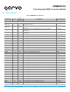
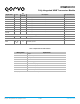
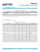
Signal Name
Pin
I/O
(Default)
Description
IC Pin Reference
P0.07
40
DIO
General purpose I/O for nRF52833 processor.
[N] P0.07
P0.27
41
DIO
General purpose I/O for nRF52833 processor.
[N] P0.27
P0.31
42
DIO
General purpose I/O for nRF52833 processor.
[N] P0.31
P0.30
43
DIO
General purpose I/O for nRF52833 processor.
[N] P0.30
DW_GPIO3
44
DIO
General purpose I/O for DW3110 transceiver.
[D] GPIO3
DW_GPIO2
45
DIO
General purpose I/O for DW3110 transceiver.
[D] GPIO2
P0.02
46
DIO
General purpose I/O for nRF52833 processor.
[N] P0.02
RESET
(P0.18)
47
DIO
General purpose I/O for nRF52833 processor. Active-low reset input.
[N] nRESET
Power Supplies
VDD
12
P
3 V supply pin.
Ground
GND
1, 11,
21, 38,
48
G
Common ground.
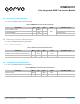
Table 3: Explanation of Abbreviations
Abbreviation
Explanation
I
Input
IO
Input / Output
O
Output
G
Ground
P
Power Supply
PD
Power Decoupling
O-L
Defaults to output, low level after reset
O-H
Defaults to output, high level after reset
I
Defaults to input.
Note: Any signal with the suffix ‘n’ indicates an active low signal.