
Specifications


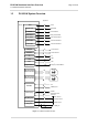
Table Of Contents
- Contents
- Tables
- Figures
- 1 Introduction
- 2 Interface Characteristics
- 3 Operating Characteristics
- 4 Mechanical Dimensions, Mounting and Packaging
- 5 Regulatory and Type Approval Information
- 6 Document Information

PLS63-W Hardware Interface Overview
Figures
Page 5 of 48
Figures
Figure 1: PLS63-W system overview ............................................................................ 11
Figure 2: USB circuit ..................................................................................................... 12
Figure 3: Serial interface ASC0..................................................................................... 13
Figure 4: Serial interface ASC1..................................................................................... 14
Figure 5: Module’s two UICC/SIM/USIM interfaces ...................................................... 16
Figure 6: UICC/SIM/USIM interfaces connected........................................................... 16
Figure 7: External UICC/SIM/USIM switch.................................................................... 17
Figure 8: Sample circuit for SIM interface connection via SIM switch........................... 17
Figure 9: Status signaling with LED driver .................................................................... 20
Figure 10: Power indication signal .................................................................................. 21
Figure 11: Antenna pads (bottom view) .......................................................................... 23
Figure 12: Embedded Stripline with 65µm prepreg (1080) and 710µm core .................. 24
Figure 13: Micro-Stripline on 1.0mm standard FR4 2-layer PCB - example 1 ................ 25
Figure 14: Micro-Stripline on 1.0mm Standard FR4 PCB - example 2............................ 26
Figure 15: Micro-Stripline on 1.5mm Standard FR4 PCB - example 1............................ 27
Figure 16: Micro-Stripline on 1.5mm Standard FR4 PCB - example 2............................ 28
Figure 17: Routing to application‘s RF connector ........................................................... 29
Figure 18: PLS63-W evaluation board layer table........................................................... 29
Figure 19: Supply voltage for active GNSS antenna....................................................... 30
Figure 20: ESD protection for passive GNSS antenna ................................................... 31
Figure 21: Decoupling capacitor(s) for BATT+................................................................ 32
Figure 22: PLS63-W– top and bottom viewDimensions of
PLS63-W (all dimensions in mm)................................................................... 34
Figure 23: Dimensions of PLS63-W (all dimensions in mm)........................................... 35
Figure 24: Dimensions of PLS63-W (keepout area recommended)................................ 36
Figure 25: Reference equipment for Type Approval ....................................................... 41