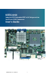
KEEX-6100 Industrial ECX Embedded SBC with 2nd generation Intel® core i3/i5/i7 processor User’s Guide KEEX-6100 User’s Manual I
Contact Info: Quanmax Inc. 4F, No. 415, Ti-Ding Blvd. Sec. 2NeiHu District, Taipei 114Taiwan Tel: +886-2-2799-2789 Fax: +886-2-2799-7399 Visit our site at: www.quanmax.com © 2011 Quanmax Inc. All rights reserved. The information in this user’s guide is provided for reference only. Quanmax does not assume any liability arising out of the application or use of the information or products described herein.
Content Content Content....................................................................................................................... 3 Figures ....................................................................................................................... 5 Tables ......................................................................................................................... 6 Safety Instructions .....................................................................................
Content Chapter 5 Driver Installation................................................................................. 55 Appendix A DIO (Digital I/O) Sample Code ............................................................ 56 Appendix B WatchDog Timer Sample Code ..........................................................
Figures Figures Figure 1 Block Diagram ............................................................................. 19 Figure 2 Mechanical Dimensions ............................................................... 21 Figure 3 Jumper Connector ....................................................................... 22 Figure 4 Jumper and Connector Locations ................................................ 23 Figure 5 Rear Panel IO .............................................................................
Tables Tables Table 1 KEEX-6100 Specification............................................................... 18 Table 2 Jumper List .................................................................................... 24 Table 3 JP1 ME F/W Selection................................................................... 24 Table 4 JP2 Panel & Backlight Power Selection for LVDS2 ....................... 24 Table 5 JP3 Panel Backlight Power Selection for LVDS1...........................
Tables Table 35 DIMM1 DDR3 Memory SO-DIMM Socket ................................... 33 Table 36 FAN1 CPU FAN Wafer................................................................. 33 Table 37 FP1 Front Panel 1 Pin Header .................................................... 33 Table 38 FP2 Front Panel 2 Pin Header .................................................... 33 Table 39 IR1 IrDA Pin Header ....................................................................
Safety Instructions Safety Instructions Before You Begin Before handling the product, read the instructions and safety guidelines on the following pages to prevent damage to the product and to ensure your own personal safety. Refer to the “Advisories” section in the Preface for advisory conventions used in this user’s guide, including the distinction between Warnings, Cautions, Important Notes, and Notes. Always use caution when handling/operating a computer.
Safety Instructions 3. 4. Follow the guidelines provided in “Preventing Electrostatic Discharge” on the following page. Disconnect any telephone or telecommunications lines from the computer. In addition, take note of these safety guidelines when appropriate: To help avoid possible damage to system boards, wait five seconds after turning off the computer before removing a component, removing a system board, or disconnecting a peripheral device from the computer.
Safety Instructions When transporting a sensitive component, first place it in an antistatic container or packaging. Handle all sensitive components at an ESD workstation. If possible, use antistatic floor pads and workbench pads. Handle components and boards with care. Don’t touch the components or contacts on a board. Hold a board by its edges or by its metal mounting bracket. Do not handle or store system boards near strong electrostatic, electromagnetic, magnetic, or radioactive fields.
Preface Preface How to Use This Guide This guide is designed to be used as step-by-step instructions for installation, and as a reference for operation, troubleshooting, and upgrades. NOTE Driver downloads and additional information are available under Downloads on our web site: www.quanmax.com. Unpacking When unpacking, follow these steps: 1. After opening the box, save it and the packing material for possible future shipment. 2. Remove all items from the box.
Preface area (domestic environment) is likely to cause harmful interference, in which case the user will be required to correct the interference (take adequate measures) at their own expense. Changes or modifications not expressly approved by Quanmax could void the user's authority to operate the equipment.
Preface date of purchase. To reduce risk of damage, returns of product must be in a Quanmax shipping container. If the original container has been lost or damaged, new shipping containers may be obtained from Quanmax Customer Service at a nominal cost. Quanmax owns all parts removed from repaired products. Quanmax uses new and reconditioned parts made by various manufacturers in performing warranty repairs and building replacement products.
Preface properties as electrical resistance and thermal conductivity. Extreme moisture buildup inside the system can result in electrical shorts, which can cause serious damage to the system. Buildings in which climate is controlled usually maintain an acceptable level of humidity for system equipment. However, if a system is located in an unusually humid location, a dehumidifier can be used to maintain the humidity within an acceptable range.
Preface Uninterruptible Power Supply Uninterruptible power supply (UPS) systems offer the most complete protection against variations on power because they use battery power to keep the server running when AC power is lost. The battery is charged by the AC power while it is available, so when AC power is lost, the battery can provide power to the system for a limited amount of time, depending on the UPS system.
Chapter 1 Chapter 1 Introduction Overview The KEEX-6100 is an ECX Form Factor embedded single board computer (SBC) that equips the latest 2nd generation Intel® Core™ i3/i5/i7 processors with the high integration of the Intel® QM67/ HM65 chipset. Featured are DDR3 1066/1333 SO-DIMM up to 8GB, 2x 24-bit LVDS, HDMI, DP, VGA, 2x Gigabit Ethernet, 2x SATA, mini PCIe slot, 8x USB 2.0, 2x COM ports with Power Selection, HD audio and CompactFlash.
Chapter 1 Product Specifications Model Name KEEX-6100 Form Factor ECX (146mm x 105mm) Processor 2nd Generation Intel core i3/i5/i7 Processors with rPGA988B package Memory 1x SO-DIMM, dual channel DDR3, non-ECC supported, up to 8GB ® Chipset Graphics Ethernet Audio Peripheral Support KEEX-6100---Intel QM67 Express Chipset ® KEEX-6101---Intel HM65 Express Chipset Intel HD Graphics 3000 rocessor graphics 1x VGA with DB-15 female connector 1x HDMI connector 1x DP Connector
Chapter 1 Expansion Slot 1x 1x6-pin pitch 2.00 mm wafer connector for PS/2 keyboard and mouse. 1x 1x5-pin pitch 2.54mm header for IrDA supported. 1x 1x3-pin fan connector onboard with smart fan supported. 1x 2x 5-pin pitch 2.54 mm header onboard for 8-bit DIO. 4-bit input and 4-bit output. DIO default setting is “H”.
Chapter 1 System Block Diagram Figure 1 Block Diagram KEEX-6100 User’s Manual 19
Chapter 1 Mechanical Dimensions KEEX-6100 User’s Manual 20
Chapter 1 Figure 2 Mechanical Dimensions KEEX-6100 User’s Manual 21
Chapter 2 Chapter 2 Hardware Settings Overview This chapter provides the definitions and locations of jumpers, headers, and connectors. Jumpers The product has several jumpers which must be properly configured to ensure correct operation. Figure 3 Jumper Connector For a three-pin jumper (see Figure 3), the jumper setting is designated “1-2” when the jumper connects pins 1 and 2. The jumper setting is designated “2-3” when pins 2 and 3 are connected and so on.
Chapter 2 Jumper Settings and Pin Definitions For jumper and connector locations, please refer to the diagrams below.
Chapter 2 Jumper Settings To ensure correct system configuration, the following section describes how to set the jumpers to enable/disable or change functions. For jumper descriptions, please refer to the table below.
Chapter 2 Table 5 JP3 Panel Backlight Power Selection for LVDS1 1 2 5 6 Jumper 1 Setting 1-3 3-5 2-4 4-6 2 Status Backlight Power = +12V Backlight Power = +5V Panel Power = +3.3V Panel Power = +5V Pitch:2.54mm [YIMTEX 3362*03SAGR] Table 6 JP4 Backlight Power Enable Selection for LVDS1 Jumper 1 2 5 Setting 1-3 1 2 6 Status Backlight Enable Voltage = +3.3V 3-5 2-4 Backlight Enable Voltage = +5V Active High 4-6 Active Low Pitch:2.
Chapter 2 Rear Panel Pin Assignments Figure 5 Rear Panel IO Table 11 Rear Panel Connector List Label CN9 CN10 DP1 HDMI1 VGA1 Function LAN1 & USB2.0 Port 0,1 Connector LAN2 & USB2.0 Port 8,9 Connector Display Port Connector HDMI Connector DB-15 VGA Connector Table 12 CN9 LAN1 & USB 2.
Chapter 2 Table 14 DP1 Display Port Connector Pin 1 2 3 4 5 6 7 8 9 10 Signal TX0+ GND TX0TX1+ GND TX1TX2+ GND TX2TX3+ Pin 11 12 13 14 15 16 17 18 19 20 Signal GND TX3GND GND AUX+ GND AUXHPD GND PWR [WIN WIN WDPE-20F3L1BU3] Table 15 HDMI1 HDMI Connector Pin Signal 1 TMDS Data2+ 2 Ground 3 TMDS Data2– 4 TMDS Data1+ 5 Ground 6 TMDS Data1– 7 TMDS Data0+ 8 Ground 9 TMDS Data0– 10 TMDS Clock+ 11 Ground 12 TMDS Clock– 13 Reserved 14 Reserved 15 DDC_CLK 16 DDC_DATA 17 Ground 18 +5 V Power 19 Hot Plug Detect [
Chapter 2 Main Board Pin Assignments Table 17 Internal Connector List Label ATX1 BAT1 BZ1 CFD1 COM1 COM2 CN1 CN2 CN3 CN4 CN5 CN6 CN7 CN8 CN12 CN13 CN14 CN20 DIMM1 FAN1 FP1 FP2 IR1 LVDS1 LVDS2 MPCIE1 SATA1 SATA2 Function +12V Power Input Connector CR2032 Battery Power Input Wafer Onboard Buzzer CF Type II Connector RS-232/422/485 Port 1 Wafer RS-232 Port 2 Wafer Digital Input / Output Pin Header SATA HDD Power Output Wafer Backlight Power Output Wafer for LVDS1 SIM Interface Wafer for MPCIE1 USB2.
Chapter 2 Table 20 CFD1 CF Type II Connector Signal Name GND IDE Data 3 IDE Data 4 IDE Data 5 IDE Data 6 IDE Data 7 IDE Chip select 1# GND GND GND GND GND +5V GND GND GND GND SDA2 IDE Address 1 IDE Address 0 IDE Data 0 IDE Data 1 IDE Data 2 IOIS16# GND Pin 1 2 3 4 5 6 7 8 9 10 11 12 13 14 15 16 17 18 19 20 21 22 23 24 25 Pin 26 27 28 29 30 31 32 33 34 35 36 37 38 39 40 41 42 43 44 45 46 47 48 49 50 Signal Name GND IDE Data 11 IDE Data 12 IDE Data 13 IDE Data 14 IDE Data 15 IDE Chip select 3# GND IDEIOR#
Chapter 2 Table 21 COM1 RS-232/422/485 Port 1 Wafer Pin RS-232 RS-422 1 DCD TX2 DSR N/A 3 RXD RX+ 4 RTS N/A 5 TXD TX+ 6 CTS N/A 7 DTR RX8 RI N/A 9 GND GND 10 +5V +5V Pitch:1.25mm [Pinrex 712-73-10TWB0] Half Duplex RS-485 Full Duplex RS-485 DATAN/A N/A N/A DATA+ N/A N/A N/A GND +5V TXN/A RX+ N/A TX+ N/A RXN/A GND +5V Table 22 COM2 RS-232 Port 2 Wafer Pin 1 2 3 4 5 6 7 8 9 10 Signal Name DCD DSR RXD RTS TXD CTS DTR RI GND +5V Pitch:1.
Chapter 2 Table 25 CN3 Backlight Power Output Wafer for LVDS1 Pin 1 2 3 4 5 6 7 Signal Name BL_ADJ_PWM * BL_ADJ_VOL * GND +5V / +12V ** +5V / +12V ** GND BL_EN*** Pitch:1.25mm [YIMTEX 501MW1X07MTR-1R] *:BL_ADJ can be setting in BIOS setup. **:Backlight Power can be selected by JP3. ***:BL_EN can be selected by JP4. Table 26 CN4 SIM Interface Wafer for MPCIE1 Pin 1 2 3 4 5 6 Signal Name UIM_PWR UIM_DATA UIM_RESET UIM_VPP UIM_CLK GND Pitch:1.25mm [Pinrex 712-73-06TWB0] Table 27 CN5 USB 2.
Chapter 2 Table 29 CN7 S/PDIF Pin Header Pin 1 2 3 4 1 4 Signal Name S/PDIF Input GND S/PDIF Output GND Pitch:2.54mm [YIMTEX 3321*04SAGR(6T)] Table 30 CN8 Audio Pin Header 1 2 11 12 Pin 1 3 5 7 9 11 Signal Name MIC_IN_L MIC_IN_JD LINE_IN_L LINE_IN_JD LINE_OUT_L LINE_OUT_JD Pin 2 4 6 8 10 12 Signal Name MIC_IN_R GND LINE_IN_R GND LINE_OUT_R GND Pitch:2.54mm [PINREX 212-92-06GB01] Table 31 CN12 Left Channel 2W Audio AMP Output Wafer Pin 1 Signal Name Speaker+ 2 Speaker- Pitch:2.
Chapter 2 Table 34 CN20 Keyboard & Mouse Wafer Pin 1 2 3 4 5 6 Signal Name MSCLK VCC MSDAT* KBDAT GND KBCLK Pitch:2.0mm [YIMTEX 503PW1*06STR] Table 35 DIMM1 DDR3 Memory SO-DIMM Socket Height: 7.0mm [LINKTEK DDRRK-20401-TP7B] Table 36 FAN1 CPU FAN Wafer Pin 1 2 3 1 2 Signal GND +12V* FAN_RPM 3 *: PWM Fan control supported.
Chapter 2 Table 40 LVDS1 Primary 24-bit, 2-channel LVDS Panel Connector Pin 1 2 3 4 5 6 7 8 9 10 11 12 13 14 15 Signal Name LVDS_A0LVDS_A0+ LVDS_A1LVDS_A1+ LVDS_A2LVDS_A2+ GND LVDS_ACLKLVDS_ACLK+ LVDS_A3-/NC LVDS_A3+/NC LVDS_B0LVDS_B0+ GND LVDS_B1- Pin 16 17 18 19 20 21 22 23 24 25 26 27 28 29 30 Signal Name LVDS_B1+ GND LVDS_B2LVDS_B2+ LVDSBCLKLVDS_BCLK+ LVDS_B3-/NC LVDS_B3+/NC GND DDC_DATA VDDEN DDC_CLK +3.3V / +5V * +3.3V / +5V * +3.3V / +5V * Pitch:1.
Chapter 2 Table 42 MPCIE1 Mini-PCIE Express v 1.2 Socket Signal WAKE# Reserved Reserved CLKREQ# Ground REFCLKREFCLK+ Ground Reserved Reserved Ground PERn0 PERp0 Ground Ground PETn0 PETp0 Ground Ground +3.3VSB +3.3VSB Ground Reserved Reserved Reserved Reserved Pin 1 3 5 7 9 11 13 15 17 19 21 23 25 27 29 31 33 35 37 39 41 43 45 47 49 51 Pin 2 4 6 8 10 12 14 16 18 20 22 24 26 28 30 32 34 36 38 40 42 44 46 48 50 52 Signal +3.3VSB Ground +1.
Chapter 2 Table 43 SATA1 Serial ATA Port 0 Connector Pin 1 2 3 4 5 6 7 Signal Name GND TX+ TXGND RXRX+ GND [FOXCONN LD1807V-S52U] Table 44 SATA2 Serial ATA Port 1 Connector Pin Signal Name 1 GND 2 TX+ 3 TX4 GND 5 RX6 RX+ 7 GND [FOXCONN LD1807V-S52U] KEEX-6100 User’s Manual 36
Chapter 3 Chapter 3 System Installation Expansion Interfaces 1x full size mini-PCIe slot supported 1x connector onboard for SIM card signals supported NOTE When adding or removing expansion cards, make sure that you unplug the power supply first. Meanwhile, read the documentation for the expansion card to configure any necessary hardware or software settings for the expansion card, such as jumpers, switches or BIOS configuration.
Chapter 3 4. 5. Fully insert the module into the socket until a “click” is heard. Press down on the SO-DIMM so that the tabs of the socket lock on both sides of the module Figure 7 Press down on the SO-DIMM Memory Module to lock it in place Removing a DIMM: To remove the SO-DIMM, use your fingers or a small screwdriver to carefully push away the tabs that secure either side of the SO-DIMM. Lift it out of the socket. Make sure you store the SO-DIMM in an anti-static bag.
Chapter 4 Chapter 4 AMI BIOS Setup Overview This chapter provides a description of the AMI BIOS. The BIOS setup menus and available selections may vary from those of your product. For specific information on the BIOS for your product, please contact Quanmax. NOTE: The BIOS menus and selections for your product may vary from those in this chapter.
Chapter 4 Main Menu The BIOS Setup is accessed by pressing the DEL key after the Power-On Self-Test (POST) memory test begins and before the operating system boot begins. Once you enter the BIOS Setup Utility, the Main Menu will appear on the screen. The Main Menu provides System Overview information and allows you to set the System Time and Date. Use the “<” and “>” cursor keys to navigate between menu screens.
Chapter 4 Advanced Menu Table 46 Advanced Menu BIOS SETUP UTILITY Main Advanced Boot Onboard LAN1 Controller Onboard LAN1 Boot Onboard LAN2 Controller Onboard LAN2 Boot Audio Controller Security [Enabled] [Disabled] [Enabled] [Disabled] [Enabled] >Display Configuration >Super IO Configuration >Power Management Configuration >CPU Advanced Configuration >Trusted Computing >SATA Configuration >Intel TXT(LT) Configuration >AMT Configuration >USB Configuration >H/W Monitor Server Mgmt Select Scree
Chapter 4 Table 47 Advanced Menu – Display Configuration BIOS SETUP UTILITY Main Advanced Boot Security Server Mgmt Display Configuration Primary Display Internal Graphics Aperture Size DVMT Pre-Allocated DVMT Total Gfx Mem [Auto] [Auto] [256 MB] [64M] [256 M] IGFX – Boot Type IGFX – 2nd Boot Type Active LVDS1 LVDS1 Panel Type LVDS1 Panel Color Depth LVDS2 Panel Type LVDS1 Backlight Control – Voltage LVDS2 Backlight Control – Voltage [VBIOS Default] [Disabled] [Disabled] [VBIOS Default] [18 bit] [1
Chapter 4 LVDS2 Panel Type Options: 640x480 18Bit 1CH, 800x480 18Bit 1CH, 800x600 18Bit 1CH, 1024x768 18Bit 1CH, 1440x900 18Bit 2CH, 1600x900 18Bit 2CH, 800x480 24Bit 1CH, 800x600 24Bit 1CH, 1024x768 24Bit 1CH, 1280x1024 24Bit 2CH, 1366x768 24Bit 1CH, 1366x768 24Bit 2CH, 1440x900 24Bit 2CH, 1600x1200 24Bit 2CH, 1920x1080 24Bit 2CH, 1920x1200 24Bit 2CH LVDS1 Backlight Control – Voltage Options: 0.0V, 0.5V, 1.0V, 1.5V, 2.0V, 2.5V, 3.0V, 3.5V, 4.0V, 4.5V, 5.0V LVDS2 Backlight Control – Voltage Options: 0.
Chapter 4 Table 49 Advanced Menu – Super IO Configuration – Serial Port 1 Configuration BIOS SETUP UTILITY Main Advanced Boot Security Serial Port 1 Configuration Save & Exit Enable or Disable Serial Port (COM) Serial Port Device Settings [Enabled] IO=3F8h; IRQ=4; Change Settings Serial Port 1 Type [Auto] [RS232] Select Screen ↑↓ Select Item Enter: Select +- Change Opt. F1: General Help F2: Previous Values F3: Optimized Defaults F4 Save & Exit ESC Exit Version 2.10.1208.
Chapter 4 Change Settings Options: Auto, IO=2F8h; IRQ=3; IO=3F8h; IRQ=3, 4, 5, 6, 7, 9, 10, 11, 12; IO=2F8h; IRQ=3, 4, 5, 6, 7, 9, 10, 11, 12; IO=3E8h; IRQ=3, 4, 5, 6, 7, 9, 10, 11, 12; IO=2E8h; IRQ=3, 4, 5, 6, 7, 9, 10, 11, 12; Device Mode Options: Standard Serial Port Mode, IrDA function, active pulse is 1.6us, IrDA function, active pulse is 3/16 bit time.
Chapter 4 Options: Disabled, Enabled Table 52 Advanced Menu –CPU Advanced Configuration BIOS SETUP UTILITY Main Advanced Boot Security CPU Advanced Configuration EIST Turbo Mode Intel ® Virtualization Tech VT-d Intel ® Hyper Treading Tech Active Processor Cores Limit CPUID Maximum Execute Disable Bit Save Exit Enable/Disable Intel ® Speed Step ™ Tech. [Enabled] [Enabled] [Disabled] [Enabled] [Enabled] [All] [Disabled] [Enabled] Select Screen ↑↓ Select Item Enter: Select +- Change Opt.
Chapter 4 Table 53 Advanced Menu –Trusted Computing BIOS SETUP UTILITY Main Advanced Boot TPM Configuration TPM SUPPORT Security Save & Exit Enable/Disable TPM support. O.S. will not show TPM. Reset of platform is required. [Disable] Current TPM Status Information TPM SUPPORT OFF Select Screen ↑↓ Select Item Enter: Select +- Change Opt. F1: General Help F2: Previous Values F3: Optimized Defaults F4 Save & Exit ESC Exit Version 2.10.1208. Copyright (C) 2010, American Megatrends, Inc.
Chapter 4 Table 55 Advanced Menu –Intel TXT(LT) Configuration BIOS SETUP UTILITY Main Advanced Boot Security Save & Exit Intel Trusted Execution technology Configuration Intel TXT support only can be enabled / disabled if SMX enabled. And must enables the VT support prior to TXT. Secure Mode Extensions (SMX) Intel TXT(LT) Support Select Screen ↑↓ Select Item Enter: Select +- Change Opt.
Chapter 4 MEBx Selection Screen Options: Disabled, Enabled Verbose MEBx Output Options: Disabled, Enabled Hide Un-Configure ME Confirmation Options: Disabled, Enabled MEBx Debug Message Output Un-Configure ME Options: Disabled, Enabled Intel AMT Password Write Enabled Options: Disabled, Enabled AMT Wait Timer Options: 0 only ASF Options: Disabled, Enabled Activate Remote Assistance Process Options: Disabled, Enabled USB Configure Options: Disabled, Enabled PET Progress Options: Disabled, Enabled Intel AMT
Chapter 4 Table 57 Advanced Menu –USB Configuration BIOS SETUP UTILITY Main Advanced Boot Security USB Configuration USB Devices: 2 Hubs Legacy USB Support EHCI Hand-off [Enabled] [Disabled] USB hardware delays and time-out: USB transfer time-out Device reset time-out Device power-up delay [20 sec] [20 sec] [Auto] Save EHCI hand-off Options: Disabled, Enabled USB Transfer Time-Out Options: 1, 5, 10, 20 sec. Device Transfer Time-Out Options: 10, 20, 30, 40 sec.
Chapter 4 Table 58 Advanced Menu –H/W Monitor BIOS SETUP UTILITY Main Advanced Boot Security Save & PC Health Status CPU Warning Temperature CPU Shutdown Temperature CPU Smart FAN SYS Manual PWM [Disabled] [Disabled] [Disabled] 255 CPU Temperature Top Side System Temperature Bottom Side System Temperature : +99 C : +48 C : +48 C CPU Fan Speed : 5050 RPM +3.3V +VCORE +VGFX +1.05V +1.5V +5VDUAL +12V +3.3VSB : +3.296 V : +1.080 V : +0.440 V : +1.048 V : +1.493 V : +5.120 V : +11.792 V : +3.
Chapter 4 Boot Menu Table 59 Boot Menu BIOS SETUP UTILITY Main Advanced Boot Configuration Full Screen LOGO Display Setup Prompt Timeout Bootup NumLock State Boot Option Priorities Boot Option #1 Boot Security [Disabled] 1 [On] [SATA: WDC WD6402AA…] Hard Drive BBS Priorities Bootup Numlock State Options: On, Off Boot Option #1 Options: SATA: WDC WD6402AAEX-00Z3A0, Disabled Hard Drive BBS Priorities Boot Option #1: SATA: Maxtor 6L120M0, Disabled KEEX-6100 User’s Manual 52 & Exit Enables or D
Chapter 4 Security Menu Table 60 Security Menu BIOS SETUP UTILITY Main Advanced Boot Security Password Description Save & Exit Set Setup Administrator Password If ONLY the Administrator’s password is set, then this only limits access to Setup and is only asked for when entering Setup If ONLY the User’s password is set, then this is a power on password and must be entered to boot or enter Setup.
Chapter 4 Save Changes and Exit Exit system setup after saving the changes. Once you are finished making your selections, choose this option from the Exit menu to ensure the values you selected are saved to the CMOS RAM. The CMOS RAM is sustained by an onboard backup battery and stays on even when the PC is turned off. When you select this option, a confirmation window appears. Select [Yes] to save changes and exit. Discard Changes and Exit Exit system setup without saving any changes.
Chapter 5 Chapter 5 Driver Installation If your KEMX-6000 does not come with an operating system pre-installed, you will need to install an operating system and the necessary drivers to operate it. After you have finished assembling your system and connected the appropriate power source, power it up using the power supply and install the desired operating system. You can download the drivers for the KEEX-6100 from the Quanmax website at www.quanmax.com and install as instructed there.
Appendix A Appendix A DIO (Digital I/O) Sample Code //*************************************************************** //KEEX-6100 DOS DIO sample program //Please compile with Turbo C 3.
Appendix A //DO_2 is bit 5 //DO_3 is bit 6 outp(0x539,RetVal); RetVal=inp(0x53B);//IO Port: 0x53B RetVal=(RetVal|0x01);//DO_4 is bit 0 outp(0x53B,RetVal); system("pause"); //Reading DI_1~4 RetVal=inp(0x50C);//IO Port: 0x50C RetVal=(RetVal&0x3C);//DI_1 is bit 2 //DI_2 is bit 3 //DI_3 is bit 4 //DI_4 is bit 5 printf("DI_= %d\n",RetVal); system("pause"); return 0; } KEEX-6100 User’s Manual 57
Appendix B Appendix B WatchDog Timer Sample Code //============================================ //KEEX-6100 DOS Watchdog sample program //Please compile with Turbo C 3.0 to utilized the program //============================================ #include int main() { int value; //Initialized the WDT program outp(0x2E,0x87); outp(0x2E,0x87); //Setting Logical Device Number to 0x07 outp(0x2E,0x07); outp(0x2F,0x07); //0xF5 bit6 //If watchdog timeout event occurs, this bit will be set to 1.
Appendix B outp(0x2E,0xF0); outp(0x2F,0x81);//bit7 WDTRST# output is enabled return 0; } KEEX-6100 User’s Manual 59