
User Manual

UANTA COMPUTER INC. CNBU/1KU3
________________________________________________________________________________________
____________________________________________________________________________
1KU Product Specification Rev. 2B Page: 8
- Quanta Confidential -
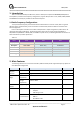
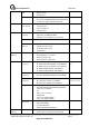
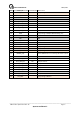
4.2 Electrical Specification
4.2.1 Power Specification
Name
Pin
Description
Min
Typ
Max
Unit
VCC_VBAT
2, 24, 39, 41, 52
VCC power
3.4
3.8
4.2
V
VCC_USIM/ 3.0V
8
USIM power output 3.0V
2.7
3
3.3
V
VCC_USIM/ 1.8V
8
USIM power output 1.8V
1.62
1.8
1.98
V
V_IH
1.8V Digital I/O
input high voltage
1.62
1.8
1.98
V
V_IL
1.8V Digital I/O
input low voltage
0
0.1
0.45
V
V_OH
1.8V Digital I/O
output high voltage
1.62
1.8
1.98
V
V_OL
1.8V Digital I/O
output low voltage
0
0.1
0.45
V
PERST_N
22
Hardware Reset (PU)
-0.3
0
0.6
V
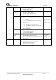
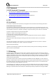
4.2.2 Pin Assignment
Pin
Name
Power Level
Description
1
POWER_ON_OFF
1.8V
Modem power on/off
2
VCC_VBAT
4.2~3.4V
Supply voltage for Modem
3
VREG_MSME_1V8
1.8V
Supply voltage for JTAG function
4
GND
GND
5
MDM_JTAG_PS_HOLD
JTAG Function
6
WAKE_UP
1.8V
Wake-up Modem
7
MDM_JTAG_RESET_N
JTAG Function
8
VREG_RUIM1
1.8/3V
SIM function
9
GND
GND
10
UIM1_DATA
SIM function
11
PA_state
1.8V
Indicate 3G/LTE/EVDO PA state for coexistence
12
UIM1_CLK
SIM function
13
(1)MDM_RTCK
or
(2)TCXO_GPS_EN
(1)JTAG Function
or
(2)Enable the output of TCXO(19.2MHz) so as to be used
by GPS of main system
*Depends on system how to design
14
UIM1_RESET
SIM function
15
GND
GND
16
UIM1_DET
Detection of SIM insertion/plug-out
17
(1)MDM_TCK
or
(2)TCXO_GPS
(1)JTAG Function
or
(2)TCXO(19.2MHz) output for GPS of main system
*Depends on system how to design
18
GND
GND
19
MDM_TMS
JTAG Function
20
Suspend
1.8V
Trigger Modem to enter into sleep mode
21
GND
GND
22
PM28_RESET_N
Reset Modem