
Specifications

5102ch02.fm Draft Document for Review May 12, 2014 12:46 pm
30 IBM Power System S822 Technical Overview and Introduction
The innovation of using eDRAM on the POWER8 processor die is significant for
several reasons:
Latency improvement
A six-to-one latency improvement occurs by moving the L3 cache on-chip compared to L3
accesses on an external (on-ceramic) ASIC.
Bandwidth improvement
A 2x bandwidth improvement occurs with on-chip interconnect. Frequency and bus sizes
are increased to and from each core.
No off-chip driver or receivers
Removing drivers or receivers from the L3 access path lowers interface requirements,
conserves energy, and lowers latency.
Small physical footprint
The performance of eDRAM when implemented on-chip is similar to conventional SRAM
but requires far less physical space. IBM on-chip eDRAM uses only a third of the
components that conventional SRAM uses, which has a minimum of six transistors to
implement a 1-bit memory cell.
Low energy consumption
The on-chip eDRAM uses only 20% of the standby power of SRAM.
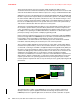
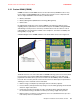
2.1.6 L4 cache and memory buffer
POWER8 processor-based systems introduce an additional level in memory hierarchy. The
L4 cache is implemented together with the memory buffer in the Custom DIMM (CDIMM).
Each memory buffer contains 16 MB of L4 cache, and on a Power S822 you can have up to
128 MB of L4 cache.
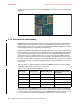
Figure 2-7 shows a picture of the memory buffer, where you can see the 16 MB L4 cache, as
well as processor links and memory interfaces.
Figure 2-7 Memory buffer chip
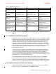
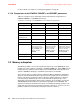
Table 2-3 on page 31 shows a comparison of the different levels of cache in the POWER7,
POWER7+ and POWER8 processors.