
Specifications

Chapter 2. Architecture and technical overview 31
Draft Document for Review May 12, 2014 12:46 pm 5102ch02.fm
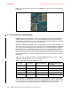
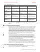
Table 2-3 POWER8 cache hierarchy
For more information on the POWER8 memory subsystem, see 2.2, “Memory subsystem” on
page 34.
2.1.7 Hardware transactional memory
Transactional memory is an alternative to lock-based synchronization. It attempts to simplify
parallel programming by grouping read and write operations and running them like a single
operation. Transactional memory is like database transactions where all shared memory
accesses and their effects are either committed all together or discarded as a group. All
threads can enter the critical region simultaneously. If there are conflicts in accessing the
shared memory data, threads try accessing the shared memory data again or are stopped
without updating the shared memory data. Therefore, transactional memory is also called a
lock-free synchronization. Transactional memory can be a competitive alternative to
lock-based synchronization.
Transactional memory provides a programming model that makes parallel programming
easier. A programmer delimits regions of code that access shared data and the hardware
executes these regions atomically and in isolation, buffering the results of individual
instructions, and retrying execution if isolation is violated. Generally, transactional memory
allows programs to use a programming style that is close to coarse-grained locking to achieve
performance that is close to fine-grained locking.
Most implementations of transactional memory are based on software. The POWER8
processor-based systems provide a hardware-based implementation of transactional
memory, that is more efficient than the software implementations and requires no interaction
with the processor core, therefore allowing the system to operate in maximum performance.
2.1.8 Coherent Accelerator Processor Interface
The Coherent Accelerator Interface Architecture (CAIA) defines a coherent accelerator
interface structure for attaching special to the POWER systems.
Cache POWER7 POWER7+ POWER8
L1 instruction cache:
Capacity/associativity
32 KB, 4-way 32 KB, 4-way 32 KB, 8-way
L1 data cache:
Capacity/associativity
bandwidth
32 KB, 8-way
2 16 B reads or
1 16 B writes per cycle
32 KB, 8-way
2 16 B reads or
1 16 B writes per cycle
64 KB, 8-way
4 16 B reads or
1 16 B writes per cycle
L2 cache:
Capacity/associativity
bandwidth
256 KB, 8-way
Private
32 B reads and 16 B writes
per cycle
256 KB, 8-way
Private
32 B reads and 16 B writes
per cycle
512 KB, 8-way
Private
64 B reads and 16 B writes
per cycle
L3 cache:
Capacity/associativity
bandwidth
On-Chip
4 MB/core, 8-way
16 B reads and 16 B writes
per cycle
On-Chip
10 MB/core, 8-way
16 B reads and 16 B writes
per cycle
On-Chip
8 MB/core, 8-way
32 B reads and 32 B writes
per cycle
L4 cache:
Capacity/associativity
bandwidth
N/A N/A On-Chip
16 MB/buffer chip, 16-way
Up to 8 buffer chips per
socket