
User's Manual


GV5
0
TRA
C
2.3
.
The
L-li
n
foll
o
Tab
l
Ind
e
1
2
3
4
5
6
7
8
9
10
11
12
0
0UserManu
a
C
GV500UM00
1
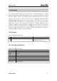
. Interfac
e
GV500 has
a
n
e and J185
o
wing figure:
l
e 4: Descrip
t
e
x D
e
P
W
L
_
H
S
M
J1
K
_
H
S
G
N
G
N
M
J1
S
W
a
l
1
e
Definitio
a
n OBD II c
o
0 bus. The
Figure
2
t
ion of OBD
I
e
scription
W
R
_
line
S
_CAN_L
S_CAN_L
850_BUS-
_
Line
S
_CAN_H
N
D
N
D
S_CAN_H
850_BUS+
W
_CAN
n
o
nnector. It c
o
sequence a
n
2
. The
O
I
I Connectio
n
C
E
x
L
H
M
J
1
K
H
P
o
P
o
M
J
1
S
W
o
ntains pow
e
n
d definition
O
BD II conn
n
s
C
omment
x
ternal DC p
line of ISO
9
H
S_CAN_H l
i
M
S_CAN_L l
i
1
850 Bus ne
g
K
line of ISO
9
H
S_CAN_H l
i
o
wer and dig
o
wer and dig
M
S_CAN_H
l
1
850 Bus po
s
W
_CAN of I
e
r supply and
of the OB
D
ector on th
ower input,
8
9
141, ISO 91
4
i
ne of ISO 11
i
ne of ISO 1
1
g
ative line of
9
141, ISO 9
1
i
ne of ISO 11
ital ground
ital ground
l
ine of ISO 1
1
s
itive line of
J
SO 11898 a
n
interfaces o
f
D
II connec
t
e GV500
8
-32V
4
1-2 and IS
O
898,J1939 a
n
898 and ISO
J
1850 PWM
41-2 and IS
O
898,J1939 a
n
1
898 and IS
O
J
1850 PWM
a
n
d ISO 15765
f
CAN bus,
K
t
or are sho
w
O
14230
n
d ISO 1576
5
O
15765
and J1850
V
O
14230
n
d ISO 1576
5
O
15765
and J1850 V
P
5
‐8‐
K
-line,
w
n in
5
V
PW
5
P
W