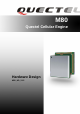
M80 Hardware Design M80 Quectel Cellular Engine Hardware Design M80_HD_V1.2 M80_HD_V1.
M80 Hardware Design Document Title M80 Hardware Design Revision 1.2 Date 2012-07-23 Status Released Document Control ID M80_HD_V1.2 General Notes Quectel offers this information as a service to its customers, to support application and engineering efforts that use the products designed by Quectel. The information provided is based upon requirements specifically provided for customers of Quectel.
M80 Hardware Design Contents Contents ............................................................................................................................................ 3 Table Index........................................................................................................................................ 6 Figure Index ...................................................................................................................................... 7 0. Revision history ..........
M80 Hardware Design 3.9.4. Level match ............................................................................................................. 49 3.10. Audio interfaces .............................................................................................................. 52 3.10.1. Decrease TDD noise and other noise .................................................................... 53 3.10.2. Microphone interfaces design.......................................................................
M80 Hardware Design Appendix A: GPRS coding schemes............................................................................................... 89 Appendix B: GPRS multi-slot classes............................................................................................. 90 M80_HD_V1.
M80 Hardware Design Table Index TABLE 1: RELATED DOCUMENTS ................................................................................................... 10 TABLE 2: TERMS AND ABBREVIATIONS ....................................................................................... 11 TABLE 3: MODULE KEY FEATURES ................................................................................................ 16 TABLE 4: CODING SCHEMES AND MAXIMUM NET DATA RATES OVER AIR INTERFACE ..
M80 Hardware Design Figure Index FIGURE 1: MODULE FUNCTIONAL DIAGRAM ............................................................................. 19 FIGURE 2: PIN ASSIGNMENT ............................................................................................................ 21 FIGURE 3: RIPPLE IN SUPPLY VOLTAGE DURING TRANSMITTING BURST ........................... 31 FIGURE 4: REFERENCE CIRCUIT OF THE VBAT INPUT ..............................................................
M80 Hardware Design FIGURE 42: RI BEHAVIOR OF DATA CALLING AS A RECEIVER ................................................ 68 FIGURE 43: RI BEHAVIOR AS A CALLER ........................................................................................ 68 FIGURE 44: RI BEHAVIOR OF URC OR SMS RECEIVED .............................................................. 69 FIGURE 45: REFERENCE DESIGN FOR NETLIGHT .......................................................................
M80 Hardware Design 0. Revision history Revision Date Author Description of change 1.0 2011-12-20 Ray XU Initial. 1.1 2012-02-03 Ray XU 1. 2. 3. 4. 1.2 2012-07-20 Baly BAO 1. Deleted the USB interface. 2. Deleted the camera interface. M80_HD_V1.2 Updated PCM interface. Updated SD interface. Updated charging interface. Updated timing of turning on the module.
M80 Hardware Design 1. Introduction This document defines the M80 module and describes the hardware interface of M80 which are connected with the customer application and the air interface. This document can help customers quickly understand module interface specifications, electrical and mechanical details. Associated with application notes and user guide, customers can use M80 module to design and set up mobile applications easily. 1.1.
M80 Hardware Design 1.2.
M80 Hardware Design Li-Ion Lithium-Ion MO Mobile Originated MS Mobile Station (GSM engine) MT Mobile Terminated PAP Password Authentication Protocol PBCCH Packet Switched Broadcast Control Channel PCB Printed Circuit Board PDU Protocol Data Unit PPP Point-to-Point Protocol RF Radio Frequency RMS Root Mean Square (value) RTC Real Time Clock RX Receive Direction SIM Subscriber Identification Module SMS Short Message Service TDMA Time Division Multiple Access TE Terminal Equip
M80 Hardware Design 1.3. Directives and standards The M80 module is designed to comply with the FCC statements. FCC ID: XMR201208M80. The Host system using M80, should have label indicated FCC ID: XMR201208M80. 1.3.1. FCC Statement 1. 2. This device complies with Part 15 of the FCC rules. Operation is subject to the following conditions: a) This device may not cause harmful interference. b) This device must accept any interference received, including interference that may cause undesired operation.
M80 Hardware Design The following list of antenna is indicating the maximum permissible antenna gain. Type Maximum Gain (850Hz/900Hz) Maximum Gain (1800Hz/1900Hz) Impedance External Antenna Monopole 0.5dBi 2dBi 50Ω Vehicular antenna 0.5dBi 2dBi 50Ω Internal Antenna Monopole 0.5dBi 2dBi 50Ω PIFA 0.5dBi 2dBi 50Ω FPC 0.5dBi 2dBi 50Ω PCB 0.5dBi 2dBi 50Ω 1.4.
M80 Hardware Design Your cellular terminal or mobile receives and transmits radio frequency energy while switched on. RF interference can occur if it is used close to TV set, radio, computer or other electric equipment. Road safety comes first! Do not use a hand-held cellular terminal or mobile while driving a vehicle, unless it is securely mounted in a holder for hands-free operation. Before making a call with a hand-held terminal or mobile, park the vehicle.
M80 Hardware Design 2. Product concept M80 is a Quad-band GSM/GPRS engine that works at frequencies of GSM850MHz, GSM900MHz, DCS1800MHz and PCS1900MHz. The M80 features GPRS multi-slot class 12 and supports the GPRS coding schemes CS-1, CS-2, CS-3 and CS-4. For more details about GPRS multi-slot classes and coding schemes, please refer to Appendix A and Appendix B. With a tiny profile of 23mm×25mm ×2.
M80 Hardware Design Temperature range Normal operation: -35°C ~ +80°C Restricted operation: -45°C ~ -35°C and +80°C ~ +85°C 1) Storage temperature: -45°C ~ +90°C DATA GPRS: GPRS data downlink transfer: max. 85.6 kbps GPRS data uplink transfer: max. 85.
M80 Hardware Design Firmware upgrade Firmware upgrade via UART Port Antenna interface Connected to antenna pad with 50 Ohm impendence control 1)When the module exceeds the temperature range, the deviations from the GSM specification may occur. For example, the frequency error or the phase error will be increased. Table 4: Coding schemes and maximum net data rates over air interface Coding scheme 1 Timeslot 2 Timeslot 4 Timeslot CS-1: 9.05kbps 18.1kbps 36.2kbps CS-2: 13.4kbps 26.8kbps 53.
M80 Hardware Design Charge RF PAM Power supply PMU RTC Saw PCM Turn on/off UART Transceiver SIM Baseband Engine Audio codec SD EINT 26MHz ADC 32kHz Serial Flash Indicator Figure 1: Module functional diagram 2.3. Evaluation board In order to help customer to develop applications with M80, Quectel supplies an evaluation board (EVB), RS-232 to USB cable, power adapter, earphone, antenna and other peripherals to control or test the module. For details, please refer to the document [12]. M80_HD_V1.
M80 Hardware Design 3. Application interface The module is equipped with 110 pin SMT pad and it adopts LGA package. Detailed descriptions on Sub-interfaces included in these pads are given in the following chapters: Power supply Turn on/off Charging interface RTC UART interfaces Audio interfaces SIM interface PCM interface ADC M80_HD_V1.
M80 Hardware Design 3.1. Pin RESERVED SIM_PRESENCE VRTC VDD_EXT GND GND RF_ANT GND GND GND VBAT VBAT VBAT BATSNS ISENSE CHGLDO CHGDET GATDRV 3.1.1.
M80 Hardware Design Table 5: M80 pin assignment PIN NO. PIN NAME I/O PIN NO.
M80 Hardware Design 73 CHGLDO 75 I 74 GATDRV RESERVED 76 RESERVED 77 RESERVED 78 RESERVED 79 RESERVED 80 RESERVED 81 RESERVED 82 RESERVED 83 RESERVED 84 RESERVED 85 RESERVED 86 RESERVED 87 RESERVED 88 RESERVED 89 RESERVED 90 RESERVED 91 RESERVED 92 RESERVED 93 GND 94 GND 95 RESERVED 96 RESERVED 97 RESERVED 98 RESERVED 99 RESERVED 100 RESERVED 101 RESERVED 102 RESERVED 103 RESERVED 104 RESERVED 105 RESERVED 106 RESERVED 107 RESERVED 108
M80 Hardware Design VDD_EXT 60 GND 37, 61, 62, 64, 65, 66, 93, 94 O backup battery or golden capacitor when the VBAT is supplied. VOnorm=2.8V Iout(max)= 730uA Iin=2.6~5 uA Supply 2.8V voltage for external circuit. Vmax=2.9V Vmin=2.7V Vnorm=2.8V Imax=20mA 1. If unused, keep this pin open. 2. Recommended to add a 2.2~4.7uF bypass capacitor, when using this pin for power supply. DC CHARACTERISTICS COMMENT Ground Charge interface PIN NAME PIN NO.
M80 Hardware Design NO. EMERG_ OFF 17 CHARACTERISTICS I Emergency off. Pulled down for at least 20ms, which will turn off the module in case of emergency. Use it only when normal shutdown through PWRKEY or AT command can’t perform well. VILmax=0.4V VIHmin=2.2V Vopenmax=2.8V Open drain/collector driver required in cellular device application. If unused, keep this pin open. Module indicator PIN NAME PIN NO.
M80 Hardware Design LOUDSPKP 14 positive and negative voice-band output keep these pins open. 2. Embedded amplifier of class AB internally. 3. Support both voice and ring. Net status indicator PIN NAME PIN NO. I/O DESCRIPTION DC CHARACTERISTICS COMMENT NETLIGHT 4 O Network status indication VOHmin= 0.85×VDD_EXT VOLmax= 0.15×VDD_EXT If unused, keep these pins open. PIN NAME PIN NO.
M80 Hardware Design PIN NAME PIN NO. I/O DESCRIPTION DC CHARACTERISTICS COMMENT TXD_AUX 40 O Transmit data If unused, keep these pins open. RXD_AUX 41 I Receive data VILmin=0V VILmax= 0.25×VDD_EXT VIHmin= 0.75×VDD_EXT VIHmax= VDD_EXT+0.3 VOHmin= 0.85×VDD_EXT VOLmax= 0.15×VDD_EXT PIN NAME PIN NO. I/O DESCRIPTION DC CHARACTERISTICS COMMENT SIM1_ VDD 56 O Power supply for SIM card The voltage can be selected by software automatically. Either 1.8V or 3V.
M80 Hardware Design 0.2×SIM1_VDD VOHmin= 0.9×SIM1_VDD SIM1_GND 52 SIM ground SIM_ PRESENCE 57 I SIM card detection VILmin=0V VILmax= 0.25×VDD_EXT VIHmin= 0.75×VDD_EXT VIHmax= VDD_EXT+0.3 If unused, keep these pins open. PIN NAME PIN NO. I/O DESCRIPTION DC CHARACTERISTICS COMMENT ADC0 2 I General purpose analog to digital converter. Voltage range: 0V to 2.8V If unused, keep these pins open. ADC1 1 I General purpose analog to digital converter. Voltage range: 0V to 2.
M80 Hardware Design VDD_EXT+0.3 VOHmin= 0.85×VDD_EXT VOLmax= 0.15×VDD_EXT RF interface PIN NAME PIN NO. I/O DESCRIPTION DC CHARACTERISTICS COMMENT RF_ANT 63 I/O RF antenna pad Impedance of 50Ω PIN NAME PIN NO. I/O DESCRIPTION DC CHARACTERISTICS COMMENT DOWNLOAD 3 I VILmin=0V VILmax= 0.25×VDD_EXT VIHmin= 0.75×VDD_EXT VIHmax= VDD_EXT+0.3 Keep this open. RESERVED 22~ 33, 38, 39, 44, 58, 75~ 92 95~ 110 Other interface M80_HD_V1.2 pin Keep these pins open.
M80 Hardware Design 3.2. Operating modes The table below briefly summarizes the various operating modes in the following chapters. Table 7: Overview of operating modes Mode Function Normal operation GSM/GPRS SLEEP The module will automatically go into SLEEP mode if DTR is set to high level and there is no interrupt (such as GPIO interrupt or data on UART port). In this case, the current consumption of module will reduce to the minimal level.
M80 Hardware Design 1) Use the EMERG_OFF pin only while failing to turn off the module by the command “AT+QPOWD=1” and the PWRKEY pin. Please refer to Section 3.4.2.4. 3.3. Power supply 3.3.1. Feature of GSM power The unit of GSM transmit in the wireless path is pulse string which is constructed by GSMK bit string and we call it burst. The period of burst is 4.16ms and the last time of burst is 577us. The burst current will reach 1.6A while idle current is as low as tens of milliampere.
M80 Hardware Design illustrated in Figure 4. The capacitors should be placed close to the M80 VBAT pins. The PCB traces from the VBAT pads to the power source must be wide enough to ensure that there isn’t too much voltage drop occurring in the transmitting burst mode. The width of trace should be no less than 2mm and the principle of the VBAT trace is the longer, the wider. The VBAT voltage can be measured by oscilloscope. VBAT + C1 C2 C1=100uF, C2=0.
M80 Hardware Design 3.3.4. Monitor power supply To monitor the supply voltage, you can use the “AT+CBC” command which includes three parameters: charging status, remaining battery capacity and voltage value (in mV). It returns the 0-100 percent of battery capacity and actual value measured between VBAT and GND. The voltage is automatically measured in period of 5s. The displayed voltage (in mV) is averaged over the last measuring period before the “AT+CBC” command is executed.
M80 Hardware Design PWRKEY 4.7K Turn on pulse 47K Figure 6: Turn on the module using driving circuit The other way to control the PWRKEY is using a button directly. A TVS component is indispensable to be placed nearby the button for ESD protection. When pressing the key, electrostatic strike may generate from finger. A reference circuit is shown in the following figure.
M80 Hardware Design 1 VBAT 2 EMERG_OFF (INPUT) >1s VIH > 0.6*VBAT PWRKEY (INPUT) VIL<0.1*VBAT 54ms VDD_EXT (OUTPUT) 800ms STATUS (OUTPUT) MODULE STATUS OFF BOOTING RUNNING Figure 8: Timing of turning on system ① Make sure that VBAT is stable before pulling down PWRKEY pin. The time between them is recommended 30ms. ② EMERG_OFF should be floated when it is unused Note: Customer can monitor the voltage level of the STATUS pin to judge whether the module is power-on.
M80 Hardware Design 3.4.2.1. Power down module using the PWRKEY pin Customer’s application can turn off the module by driving the PWRKEY to a low level voltage for certain time. The power-down scenario is illustrated in Figure 9. The power-down procedure causes the module to log off from the network and allows the software to save important data before completely disconnecting the power supply, thus it is a safe way.
M80 Hardware Design below: NORMAL POWER DOWN After that moment, no further AT commands can be executed. And then the module enters the POWER DOWN mode, only the RTC is still active. The POWER DOWN mode can also be indicated by STATUS pin, which is a low level voltage in this mode. Please refer to document [1] for details about the AT command “AT+QPOWD”. 3.4.2.3. Over-voltage or under-voltage automatic shutdown The module will constantly monitor the voltage applied on the VBAT, if the voltage is ≤ 3.
M80 Hardware Design EMERG_OFF 4.7K Emergency shutdown pulse 47K Figure 10: Reference circuit for EMERG_OFF by using driving circuit S1 EMERG_OFF TVS1 Close to S1 Figure 11: Reference circuit for EMERG_OFF by using button 3.4.3. Restart 3.4.3.1. Restart module using the PWRKEY pin Customer’s application can restart the module by driving the PWRKEY to a low level voltage for a certain time, which is similar to the way of turning on module.
M80 Hardware Design Delay > 0.5s Turn off PWRKEY (INPUT) Restart H Pull down the PWRKEY to turn on the module STATUS (OUTPUT) Figure 12: Timing of restarting system The module can also be restarted by the PWRKEY after emergency shutdown. 6us Pulldown > 20ms Delay>2s EMERG_OFF (INPUT) STATUS (OUTPUT) PWRKEY (INPUT) Figure 13: Timing of restarting system after emergency shutdown M80_HD_V1.
M80 Hardware Design 3.5. Charging interface M80 provides charging function for rechargeable Li-Ion or Lithium Polymer battery. It is introduced simply in this document. If you want to get more information about charging, please refer to document [13]. Table 8: Pin definition of the charging Item No. I/O Description. GATDRV 74 O Charge driving CHGLDO 73 I Charge power CHGDET 72 I Charging detect ISENSE 71 I Current sense BATSNS 70 I VBAT voltage sense 3.6.
M80 Hardware Design “AT+CFUN=1”. For detailed information about “AT+CFUN”, please refer to document [1]. 3.6.2. SLEEP mode The SLEEP mode is disabled in default software configuration. Customer’s application can enable this mode by “AT+QSCLK=1”. On the other hand, the default setting is “AT+QSCLK=0” and in this mode, the module can’t enter SLEEP mode. When “AT+QSCLK=1” is sent to the module, customer’s application can control the module to enter or exit from the SLEEP mode through pin DTR.
M80 Hardware Design 3.8. RTC backup The RTC (Real Time Clock) can be supplied by an external capacitor or battery (rechargeable or non-chargeable) through the pin VRTC. A 1.5 K resistor has been integrated in the module for current limiting. A coin-cell battery or a super-cap can be used to backup power supply for RTC. The following figures show various sample circuits for RTC backup. MODULE VRTC 1.
M80 Hardware Design Figure 17: Seiko XH414H-IV01E Charge Characteristics 3.9. Serial interfaces The module provides three serial ports: UART Port, Debug Port and Auxiliary UART Port. The module is designed as a DCE (Data Communication Equipment), following the traditional DCE-DTE (Data Terminal Equipment) connection. Autobauding function supports baud rate from 4800bps to 115200bps. The UART Port: TXD: Send data to RXD of DTE. RXD: Receive data from TXD of DTE. RTS: Requests to send.
M80 Hardware Design The Debug Port DBG_TXD: Send data to the COM port of a debugging computer. DBG_RXD: Receive data from the COM port of a debugging computer. The Auxiliary UART Port TXD_AUX: Send data to the RXD of DTE. RXD_AUX: Receive data from the TXD of DTE. The logic levels are described in the following table. Table 10: Logic levels of the UART interface Parameter Min Max Unit VIL 0 0.25×VDD_EXT V VIH 0.75×VDD_EXT VDD_EXT +0.3 V 0.15×VDD_EXT V VOL VOH V 0.
M80 Hardware Design UART Port. So far only the basic mode of multiplexing is available. Support the communication baud rates as the following: 300,600,1200,2400,4800,9600,14400,19200,28800,38400,57600,115200. The default setting is autobauding mode. Support the following baud rates for Autobauding function: 4800, 9600, 19200, 38400, 57600, 115200. The module disables hardware flow control by default. AT command “AT+IFC=2,2” is used to enable hardware flow control.
M80 Hardware Design 3.9.1.2. The connection of UART The connection between module and host using UART Port is very flexible. Three connection styles are illustrated as below. Reference design for Full-Function UART connection is shown as below when it is applied in modulation-demodulation. Module (DCE) PC (DTE) UART Port UART port TXD RXD RTS CTS DTR DCD TXD RXD RTS CTS DTR DCD RI RING GND GND Figure 18: Reference design for Full-Function UART Three-line connection is shown as below.
M80 Hardware Design reliability of the mass data communication. Module(DCE) Host (DTE) Controller TXD TXD RXD RXD RTS RTS CTS CTS GND GND Figure 20: Reference design for UART Port with hardware flow control 3.9.1.3. Software upgrade The TXD, RXD can be used to upgrade software. The PWRKEY pin must be pulled down before the software upgrade. Please refer to the following figures for software upgrade.
M80 Hardware Design 3.9.2. Debug Port Debug Port Two lines: DBG_TXD and DBG_RXD It outputs log information automatically. Debug Port is only used for software debugging and its baud rate must be configured as 460800bps. Module (DCE) Debug port Debug Computer DBG_TXD TXD DBG_RXD RXD GND GND Figure 22: Reference design for Debug Port 3.9.3.
M80 Hardware Design Host (DTE) Controller Module (DCE) TXD_AUX TXD RXD_AUX RXD GND GND Figure 23: Reference design for Auxiliary UART port 3.9.4. Level match The reference design of 3.3V level match is shown as below. If the host is a 3V system, please change the 5.6K resistor to 15K. MODULE MCU/ARM 5K6 TXD RXD RTS CTS GPIO 1K 1K 1K 1K 1K 5K6 5K6 VBAT GND RXD TXD RTS CTS DTR EINT 1K RI GPIO 1K DCD Voltage Level: 3.3V Figure 24: Level match design for 3.3V system M80_HD_V1.
M80 Hardware Design The reference design for 5V level match is shown as below. The connection of dotted line can be referred to the connection of solid line. Please pay attention to the direction of signal. Input dotted line of module should be referred to input solid line of the module. Output dotted line of module should be referred to output solid line of the module. As to the circuit below, VDD_EXT supplies power for the I/O of module, while VCC_MCU supplies power for the I/O of the MCU/ARM.
M80 Hardware Design The following circuit shows a reference design for the communication between module and PC. Since the electrical level of module is 2.8V, so a RS-232 level shifter must be used.
M80 Hardware Design 3.10. Audio interfaces The module provides two analogy input channels and three analogy output channels.
M80 Hardware Design Customer can also use “AT+CLVL” to adjust the output gain level of receiver and speaker. “AT+QECHO” is used to set the parameters for echo cancellation control. “AT+QSIDET” is used to set the side-tone gain level. For more details, please refer to document [1]. Table 13: AOUT3 output characteristics Item Condition RMS power 8ohm load VBAT=4.3v THD+N=1% 800 mW 8ohm load VBAT=3.7v THD+N=1% 700 mW 8ohm load VBAT=3.
M80 Hardware Design 3.10.2. Microphone interfaces design AIN1 and AIN2 channels come with internal bias supply for external electret microphone. A reference circuit is shown in the following figure. Close to Microphone GND GND GND Differential layout 10pF 33pF 10pF 33pF ESD ANTI MICxP Module Electret Microphone MICxN ESD ANTI 33pF 10pF GND GND GND Figure 27: Reference design for AIN1&AIN2 3.10.3.
M80 Hardware Design Close to receiver GND Differential layout 33pF 10pF Module SPK2P 22uF ESD ANTI AGND Figure 29: Handset interface design for AOUT2 Close to speaker GND Differential layout Amplifier circuit 10pF 33pF ESD ANTI 10pF 33pF ESD ANTI C1 Module SPK2P AGND C2 GND Figure 30: Speaker interface design with an amplifier for AOUT2 Texas Instrument’s TPA6205A1is recommended for a suitable differential audio amplifier. There are plenty of excellent audio amplifiers in the market.
M80 Hardware Design 3.10.4. Earphone interface design Close to Socket Differential layout GND 4.7uF 33pF MIC2N MIC2P GND GND 33pF 68R Module 22uF SPK2P 3 AGND 33pF 4 2 1 10pF Amphenol 9001-8905-050 AGND AGND GND GND GND Figure 31: Earphone interface design 3.10.5. Loud speaker interface design Close to speaker GND Differential layout 10pF 33pF 0R Module ESD ANTI LOUDSPKP 100pF 0R LOUDSPKN 10pF 33pF ESD ANTI GND Figure 32: Loud speaker interface design M80_HD_V1.
M80 Hardware Design 3.10.6. Audio characteristics Table 14: Typical electret microphone characteristics Parameter Min Typ Max Unit Working Voltage 1.2 1.5 2.0 V Working Current 200 500 uA External Microphone Load Resistance 2.
M80 Hardware Design Table 16: Pin definition of the SIM interface Name Pin Description SIM1_VDD 56 Supply power for SIM Card. Automatic detection of SIM card voltage. 3.0V±10% and 1.8V±10%. Maximum supply current is around 10mA.
M80 Hardware Design Note: Please do not use “AT+QSIMDET=1,1” which causes to initialize SIM card when Figure 33 circuit is adopted. If customer doesn’t need the SIM card detection function, keep SIM_PRESENCE open. The reference circuit using a 6-pin SIM card socket is illustrated as the following figure.
M80 Hardware Design Figure 35: Amphenol C707 10M006 512 2 SIM card holder Table 17: Pin description of Amphenol SIM card holder Name Pin Description SIM_VDD C1 SIM Card Power Supply SIM_RST C2 SIM Card Reset SIM_CLK C3 SIM Card Clock GND C5 Ground VPP C6 Not Connect SIM_DATA C7 SIM Card data I/O 3.11.3. 8 Pin SIM cassette For 8-pin SIM card holder, it is recommended to use Molex 91228. Please visit http://www.molex.com for more information. M80_HD_V1.
M80 Hardware Design Figure 36: Molex 91228 SIM card holder Table 18: Pin description of Molex SIM card holder Name Pin Description SIM_VDD C1 SIM Card Power supply SIM_RST C2 SIM Card Reset SIM_CLK C3 SIM Card Clock SIM_PRESENCE C4 SIM Card Presence Detection GND C5 Ground VPP C6 Not Connect SIM_DATA C7 SIM Card Data I/O SIM_DETECT C8 Pulled down GND with external circuit. When the tray is present, C4 is connected to C8. M80_HD_V1.
M80 Hardware Design 3.12. SD card interface The module provides SD card interface that support many types of memory, such as Memory Stick, SD/MCC card and T-Flash or Micro SD card. The following are the main features of SD card interface. Only supports 1bit serial mode. Does not support the SPI mode SD/MMC memory card. Does not support multiple SD memory cards. Does not support hot plug. Up to 26MHz data rate in serial mode. Up to 32GB maximum memory card capacity.
M80 Hardware Design Table 20: Pin name of the SD card and Micro SD card Pin NO. Pin name of SD card Pin name of T-Flash(Micro SD) card 1 CD/DATA3 DATA2 2 CMD CD/DATA3 3 VSS1 CMD 4 VDD VDD 5 CLK CLK 6 VSS2 VSS 7 DATA0 DATA0 8 DATA1 DATA1 9 DATA2 In SD card interface designing, in order to ensure good communication performance with SD card, the following design principles should be complied with. Route SD card trace as short as possible.
M80 Hardware Design 3.13. PCM interface M80 supports PCM interface. It is used for digital audio transmission between the module and the customer’s device. This interface is composed of PCM_CLK, PCM_SYNC, PCM_IN and PCM_OUT signal lines. Pulse-code modulation (PCM) is a converter that changes the consecutive analog audio signal to discrete digital signal. The whole procedure of Pulse-code modulation contains sampling, quantizing and encoding. Table 21: Pin definition of PCM interface Name Pin NO.
M80 Hardware Design 3.13.2. Timing The sample rate of the PCM interface is 8 KHz and the clock source is 256 KHz, so every frame contains 32 bits data, since M80 supports 13bit line code PCM format, the left 19 bits is invalid. M80 support short and long synchronization format. The following diagram shows the timing of short and long synchronization format. The synchronization length in long synchronization format can be programmed by software from one bit to eight bits.
M80 Hardware Design 3.13.3. Reference design As M80 only acts as a master, the module provides synchronization and clock source. The reference design is shown as below. Customer device (Slave) Module (Master) PCM_CLK PCM_SYNC PCM_OUT PCM_IN PCM_CLK PCM_SYNC PCM_IN PCM_OUT Figure 40: Reference design for PCM 3.13.4. AT command “AT+QPCMON” can configure PCM parameter. AT command format is shown as below: AT+QPCMON= mode, Sync_Type, Sync_Length, SignExtension, MSBFirst.
M80 Hardware Design 3.14. ADC The module provides two ADC to measure the value of voltage. The command “AT+QADC” can read the voltage value applied on ADC0 pin, while AT command “AT+QEADC” can read the voltage value applied on ADC1 pin. For details of this AT command, please refer to document [1]. In order to improve the accuracy of ADC, the layout of ADC should be surrounded by ground. Table 24: Pin definition of the ADC Name Pin Description ADC0 2 Analog to digital converter.
M80 Hardware Design SMS When a new SMS comes, the RI changes to LOW and holds low level for about 120 ms, then changes to HIGH. URC Certain URCs can trigger 120ms low level on RI. For more details, please refer to the document [1] If the module is used as a caller, the RI would maintain high except the URC or SMS is received. On the other hand, when it is used as a receiver, the timing of the RI is shown below. HIGH RI LOW Idle Ring Off-hook by “ATA”. On-hook by “ATH”. SMS received.
M80 Hardware Design HIGH RI 120ms LOW Idle or talking URC or SMS Received Figure 44: RI behavior of URC or SMS received M80_HD_V1.
M80 Hardware Design 3.16. Network status indication The NETLIGHT signal can be used to drive a network status indicator LED. The working state of this pin is listed in the following table. Table 27: Working state of the NETLIGHT State Module function Off The module is not running. 64ms On/ 800ms Off The module is not synchronized with network. 64ms On/ 2000ms Off The module is synchronized with network. 64ms On/ 600ms Off GPRS data transfer is ongoing. A reference circuit is shown as below.
M80 Hardware Design VBAT 300R Module 4.7K STATUS 47K Figure 46: Reference design for STATUS M80_HD_V1.
M80 Hardware Design 4. Antenna interface The Pin 63 is the RF antenna pad. The RF interface has an impedance of 50Ω. Table 29: Pin definition of the RF_ANT Name Pin Description GND 62 Ground GND 61 Ground RF_ANT 63 RF antenna pad GND 66 Ground GND 65 Ground GND 64 Ground 4.1. RF reference design The reference design for RF is shown as below. 0R RF_ANT MODULE NM NM Figure 47: Reference design for RF M80 provides an RF antenna PAD for customer’s antenna connection.
M80 Hardware Design DCS1800/PCS1900 is <1.5dB. 4.2. RF output power Table 30: The module conducted RF output power Frequency Max Min GSM850 33dBm ±2dB 5dBm±5dB EGSM900 33dBm ±2dB 5dBm±5dB DCS1800 30dBm ±2dB 0dBm±5dB PCS1900 30dBm ±2dB 0dBm±5dB Note: In GPRS 4 slots TX mode, the max output power is reduced by 2.5dB. This design conforms to the GSM specification as described in section 13.16 of 3GPP TS 51.010-1. 4.3.
M80 Hardware Design Figure 48: RF soldering sample M80_HD_V1.
M80 Hardware Design 5. Electrical, reliability and radio characteristics 5.1. Absolute maximum ratings Absolute maximum ratings for power supply and voltage on digital and analog pins of module are listed in the following table: Table 33: Absolute maximum ratings Parameter Min Max Unit VBAT -0.3 +4.73 V Peak current of power supply 0 2 A RMS current of power supply (during one TDMA- frame) 0 0.7 A Voltage at digital pins -0.3 3.3 V Voltage at analog pins -0.3 3.
M80 Hardware Design 5.3. Power supply ratings Table 35: The module power supply ratings Parameter Description Conditions Min Typ Max Unit VBAT Supply voltage Voltage must stay within the min/max values, including voltage drop, ripple, and spikes. 3.3 4.0 4.6 V Voltage drop during transmitting burst Maximum power control level on GSM850 and GSM900.
M80 Hardware Design GSM850/EGSM 9001) DCS1800/PCS19002) Peak supply current (during transmission slot) 1) 2) Maximum power control level on GSM850 and GSM900. 615/560 420/470 1.6 mA mA 1.8 A Power control level PCL 5 Power control level PCL 0 5.4. Current consumption The values of current consumption are shown as below.
M80 Hardware Design @power level #15,Typical 66mA DATA mode, GPRS ( 3 Rx, 2 Tx ) CLASS 12 GSM850 @power level #5 <550mA,Typical 435mA @power level #12,Typical 158mA @power level #19,Typical 99mA EGSM 900 @power level #5 <550mA,Typical 400mA @power level #12,Typical 150mA @power level #19,Typical 97mA DCS 1800 @power level #0 <450mA,Typical 313mA @power level #7,Typical 130mA @power level #15,Typical 92mA PCS 1900 @power level #0 <450mA,Typical 337mA @power level #7,Typical 140mA @power level #15,Typ
M80 Hardware Design @power level #19,Typical 118mA EGSM 900 @power level #5 <660mA,Typical 560mA @power level #12,Typical 215mA @power level #19,Typical 114mA DCS 1800 @power level #0 <530mA,Typical 420mA @power level #7,Typical 173mA @power level #15,Typical 97mA PCS 1900 @power level #0 <530mA,Typical 470mA @power level #7,Typical 192mA @power level #15,Typical 101mA Note: GPRS Class 12 is the default setting. The module can be configured from GPRS Class 1 to Class 12 by “AT+QGPCLASS”.
M80 Hardware Design 6. Mechanical dimensions This chapter describes the mechanical dimensions of the module. 6.1. Mechanical dimensions of module Figure 49: M80 top and side dimensions(Unit: mm) M80_HD_V1.
M80 Hardware Design Figure 50: M80 bottom dimensions(Unit: mm) M80_HD_V1.
M80 Hardware Design 6.2. Footprint one of recommendation frame line silkscreen Figure 51: Footprint one of recommendation(Unit: mm) M80_HD_V1.
M80 Hardware Design 6.3. Footprint two of recommendation frame line silkscreen Figure 52: Footprint two of recommendation(Unit: mm) Note:In order to maintain the module, keep about 3mm away between the module and other components in the host PCB. M80_HD_V1.
M80 Hardware Design 6.4. Top view of the module Figure 53: Top view of the module M80_HD_V1.
M80 Hardware Design 6.5. Bottom view of the module Figure 54: Bottom view of the module M80_HD_V1.
M80 Hardware Design 7. Storage and manufacturing 7.1. Storage M80 is distributed in vacuum-sealed bag. The restriction of storage condition is shown as below.
M80 Hardware Design 7.2. Soldering The squeegee should push the paste on the surface of the stencil that makes the paste fill the stencil openings and penetrate to the PCB. The force on the squeegee should be adjusted so as to produce a clean stencil surface on a single pass. To ensure the module soldering quality, the thickness of stencil at the hole of the module pads should be 0.13mm for M80. Figure 55: Paste application Suggest peak reflow temperature is from 235 ºC to 245ºC (for SnAg3.0Cu0.5 alloy).
M80 Hardware Design ℃ Preheat Heating Cooling 250 Liquids Temperature 217 200℃ 200 40s~60s 160℃ 150 70s~120s 100 Between 1~3℃/S 50 0 50 100 150 200 250 300 s Time(s) Figure 56: Ramp-Soak-Spike reflow profile 7.3. Packaging M80 modules are distributed in trays of 20 pieces each. This is especially suitable for the M80 according to SMT processes requirements. The trays are stored inside a vacuum-sealed bag which is ESD protected.
M80 Hardware Design Appendix A: GPRS coding schemes Four coding schemes are used in GPRS protocol. The differences between them are shown in Table 38. Table 38: Description of different coding schemes Scheme Code rate USF Pre-coded USF Radio Block excl.USF and BCS BCS Tail Coded bits Punctured bits Data rate Kb/s CS-1 1/2 3 3 181 40 4 456 0 9.05 CS-2 2/3 3 6 268 16 4 588 132 13.4 CS-3 3/4 3 6 312 16 4 676 220 15.6 CS-4 1 3 12 428 16 - 456 - 21.
M80 Hardware Design Appendix B: GPRS multi-slot classes Twenty-nine classes of GPRS multi-slot modes are defined for MS in GPRS specification. Multi-slot classes are product dependant, and determine the maximum achievable data rates in both the uplink and downlink directions. Written as 3+1 or 2+2, the first number indicates the amount of downlink timeslots, while the second number indicates the amount of uplink timeslots.
Shanghai Quectel Wireless Solutions Co., Ltd. Room 501, Building 13, No.99 Tianzhou Road, Shanghai, China 200233 Tel: +86 21 5108 6236 Mail: info@quectel.