
User's Manual
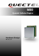

Table Of Contents
- Contents
- Table Index
- Figure Index
- 0. Revision history
- 1. Introduction
- 2. Product concept
- 3. Application interface
- 3.1. Pin
- 3.2. Operating modes
- 3.3. Power supply
- 3.4. Power on and down scenarios
- 3.5. Charging interface
- 3.6. Power saving
- 3.7. Summary of state transitions
- 3.8. RTC backup
- 3.9. Serial interfaces
- 3.10. Audio interfaces
- 3.11. SIM card interface
- 3.12. SD card interface
- 3.13. PCM interface
- 3.14. ADC
- 3.15. Behaviors of the RI
- 3.16. Network status indication
- 3.17. Operating status indication
- 4. Antenna interface
- 5. Electrical, reliability and radio characteristics
- 6. Mechanical dimensions
- 7. Storage and manufacturing
- Appendix A: GPRS coding schemes
- Appendix B: GPRS multi-slot classes

M80 Hardware Design
M80_HD_V1.2 - 4 -
3.9.4. Level match ............................................................................................................. 49
3.10. Audio interfaces .............................................................................................................. 52
3.10.1. Decrease TDD noise and other noise .................................................................... 53
3.10.2. Microphone interfaces design ................................................................................ 54
3.10.3. Receiver and speaker interface design ................................................................... 54
3.10.4. Earphone interface design ..................................................................................... 56
3.10.5. Loud speaker interface design ............................................................................... 56
3.10.6. Audio characteristics ............................................................................................. 57
3.11. SIM card interface ........................................................................................................... 57
3.11.1. SIM card application ............................................................................................. 57
3.11.2. 6 Pin SIM cassette ................................................................................................. 59
3.11.3. 8 Pin SIM cassette ................................................................................................. 60
3.12. SD card interface ............................................................................................................. 62
3.13. PCM interface ................................................................................................................. 64
3.13.1. Configuration ......................................................................................................... 64
3.13.2. Timing ................................................................................................................... 65
3.13.3. Reference design ................................................................................................... 66
3.13.4. AT command ......................................................................................................... 66
3.14. ADC ................................................................................................................................ 67
3.15. Behaviors of the RI ......................................................................................................... 67
3.16. Network status indication ................................................................................................ 70
3.17. Operating status indication .............................................................................................. 70
4. Antenna interface ........................................................................................................................ 72
4.1. RF reference design ........................................................................................................... 72
4.2. RF output power ................................................................................................................ 73
4.3. RF receiving sensitivity ..................................................................................................... 73
4.4. Operating frequencies ....................................................................................................... 73
4.5. RF cable soldering ............................................................................................................. 73
5. Electrical, reliability and radio characteristics ............................................................................ 75
5.1. Absolute maximum ratings ................................................................................................ 75
5.2. Operating temperature ....................................................................................................... 75
5.3. Power supply ratings ......................................................................................................... 76
5.4. Current consumption ......................................................................................................... 77
5.5. Electro-static discharge ..................................................................................................... 79
6. Mechanical dimensions ............................................................................................................... 80
6.1. Mechanical dimensions of module .................................................................................... 80
6.2. Footprint one of recommendation ..................................................................................... 82
6.3. Footprint two of recommendation ..................................................................................... 83
6.4. Top view of the module .................................................................................................... 84
6.5. Bottom view of the module ............................................................................................... 85
7. Storage and manufacturing ......................................................................................................... 86
7.1. Storage............................................................................................................................... 86
7.2. Soldering ........................................................................................................................... 87
7.3. Packaging .......................................................................................................................... 88