
Product Info

LTE Standard Module Series
EG91 Series Hardware Design
EG91_Series_Hardware_Design 29 / 106
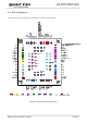
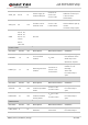
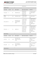
ADC0 24 AI
General-purpose
analog to digital
converter
Voltage range:
0.3V to VBAT_BB
If unused, keep it
open.
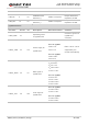
SPI Interface
Pin Name Pin No. I/O Description DC Characteristics Comment
SPI_CLK 26 DO
Clock signal of SPI
interface
V
OL
max=0.45V
V
OH
min=1.35V
1.8V power domain.
If unused, keep it
open.
SPI_MOSI 27 DO
Master output slave
input of SPI
interface
V
OL
max=0.45V
V
OH
min=1.35V
1.8V power domain.
If unused, keep it
open.
SPI_MISO 28 DI
Master input slave
output of SPI
interface
V
IL
min=-0.3V
V
IL
max=0.6V
V
IH
min=1.2V
V
IH
max=2.0V
1.8V power domain.
If unused, keep it
open.
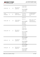
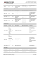
RF Interfaces
Pin Name Pin No. I/O Description DC Characteristics Comment
ANT_GNSS
49
(EG91-
NA/-NS/
-VX/-EX/
-NAX/-N
AXD/
-AUX)
AI GNSS antenna pad
50Ω impedance.
If unused, keep it
open.
The pin is defined as
ANT_DIV on
EG91-E.
ANT_DIV
49
(EG91-E)
AI
Receive diversity
antenna pad
50Ω impedance.
If unused, keep it
open.
Pin 56 is reserved on
EG91-E.
56
(EG91-
NA/-NS/
-VX/-EX/
-NAX/-N
AXD)
ANT_MAIN 60 IO Main antenna pad 50Ω impedance.
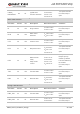
Other Pins
Pin Name Pin No. I/O Description DC Characteristics Comment
AP_READY 19 DI Application V
IL
min=-0.3V 1.8V power domain.