
Product Info


LTE Standard Module Series
EG95 Hardware Design
EG95_Hardware_Design 43 / 93
USB_DP
USB_DM
GND
USB_DP
USB_DM
GND
L1
Close to Module
R3
R4
Test Points
ESD Array
NM_0R
NM_0R
Minimize these stubs
Module
MCU
USB_VBUS
VDD
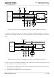
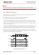
Figure 19: Reference Circuit of USB Interface
A common mode choke L1 is recommended to be added in series between the module and customer’s
MCU in order to suppress EMI spurious transmission. Meanwhile, the 0Ω resistors (R3 and R4) should be
added in series between the module and the test points so as to facilitate debugging, and the resistors are
not mounted by default. In order to ensure the integrity of USB data line signal, L1/R3/R4 components
must be placed close to the module, and also these resistors should be placed close to each other. The
extra stubs of trace must be as short as possible.
The following principles should be complied with when design the USB interface, so as to meet USB 2.0
specification.
⚫ It is important to route the USB signal traces as differential pairs with total grounding. The impedance
of USB differential trace is 90Ω.
⚫ Do not route signal traces under crystals, oscillators, magnetic devices and RF signal traces. It is
important to route the USB differential traces in inner-layer with ground shielding on not only upper
and lower layers but also right and left sides.
⚫ Pay attention to the influence of junction capacitance of ESD protection components on USB data
lines. Typically, the capacitance value should be less than 2pF.
⚫ Keep the ESD protection components to the USB connector as close as possible.
3.11. UART Interfaces
The module provides two UART interfaces: the main UART interface and the debug UART interface. The
following shows their features.
⚫ The main UART interface supports 9600bps, 19200bps, 38400bps, 57600bps, 115200bps,
230400bps, 460800bps, 921600bps and 3000000bps baud rates, and the default is 115200bps. It
supports RTS and CTS hardware flow control, and is used for AT command communication only.