
Product Info

LTE Standard Module Series
EG95 Hardware Design
EG95_Hardware_Design 58 / 93
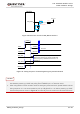
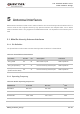
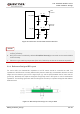
ANT_MAIN
R1 0R
C1
Module
Main
antenna
NM
C2
NM
R2 0R
C3
Diversity
antenna
NM
C4
NM
ANT_DIV
Figure 30: Reference Circuit of RF Antenna Interface
1. Keep a proper distance between the main antenna and the Rx-diversity antenna to improve the
receiving sensitivity.
2. ANT_DIV function is enabled by default. AT+QCFG="diversity",0 command can be used to disable
receive diversity.
3. Place the π-type matching components (R1/C1/C2, R2/C3/C4) as close to the antenna as possible.
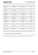
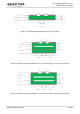
5.1.4. Reference Design of RF Layout
For user’s PCB, the characteristic impedance of all RF traces should be controlled as 50Ω. The
impedance of the RF traces is usually determined by the trace width (W), the materials’ dielectric constant,
height from the reference ground to the signal layer (H), and the space between the RF trace and the
ground (S). Microstrip and coplanar waveguide are typically used in RF layout to control characteristic
impedance. The following figures are reference designs of microstrip or coplanar waveguide with different
PCB structures.
.
Figure 31: Microstrip Line Design on a 2-layer PCB
NOTES