
Product Info

LTE-A Module Series
EG18 Hardware Design
EG18_Hardware_Design 64 / 104
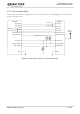
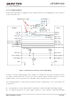
3.17.2. Endpoint Mode
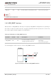
In this mode, the module is configured to act as a PCIe EP device. The following figure shows a reference
circuit of PCIe EP mode.
GND
PCIE_TX_M
PCIE_TX_P
GND
PCIE_RX_M
PCIE_RX_P
PCIE_RX_M
PCIE_RX_P
PCIE_TX_M
PCIE_TX_P
C3
C4
USB_DP
USB_DM
R1
R2
0R
0R
USB_DM
USB_DP
C1
C2
ESD Array
100nF
100nF
100nF
100nF
Module
Host
R3
R4
NM_0R
NM_0R
Test Points
Minimize these stubs
PCIE_REFCLK_P
PCIE_REFCLK_M
PCIE_REFCLK_P
PCIE_REFCLK_M
PCIE_RST_N
PCIE_CLKREQ_N
PCIE_WAKE_N
PCIE_RST_N
PCIE_CLKREQ_N
PCIE_WAKE_N
R6
100K
R5
100K
VDD_EXT
R7
NM
Figure 33: PCIe Interface Reference Circuit (EP Mode)
In order to ensure the signal integrity of PCIe interface, C1 and C2 have been placed inside the module.
C3 and C4 should be placed close to the host, and R1, R2, R3 and R4 should be placed close to the
module and also close to each other. The extra stubs of trace must be as short as possible.
The following principles of PCIe interface design should be complied with, so as to meet PCIe V2.1
specifications.
It is important to route the USB 2.0 & PCIe signal traces as differential pairs with total grounding.
For USB 2.0 signal traces,
the trace lengths should be less than 120mm, the differential data pair