
Data Sheet
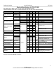
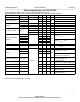
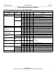


Electrical Specifications for TDD-LTE B39
Test Condition: NTC, VBATT = VCC = 3.5V, Ta = 25°C, unless otherwise specified
Signal Configuration: 3GPP TS36.101, QPSK/10MHz/12RB, 40% duty cycle, unless otherwise specified
* Noise power measured with 10MHz/1RB LTE waveform.
15
All rights reserved.
Products and Product Information are Subject to Change Without Prior Notice.
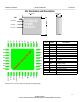
Characteristics Symbol PA_mode Min. Typ. Max. Unit Test Condition
Operating Frequency f 1880 1920 MHz
Maximum Output Power
P
out_Max_NTC
MPM
25
dBm
P
out_Max_ETC
24 ETC
Power Gain
Gain
_MPM_NTC
MPM
33 dB Pout = P
out_Max_NTC
Gain
_LPM_NTC
LPM
27 dB Pin = -35dBm
Gain
_ULPM_NTC
ULPM
24.5 dB Pin = -35dBm
Gain Variation over ETC
ΔGain_
ETC
MPM
-2 +2 dB Pout = P
out_Max_NTC,
ETC
LPM
-1.5 +1.5 dB Pin = -35dBm, ETC
ULPM
-1 +1 dB Pin = -35dBm, ETC
Adjacent Channel Leakage
Power Ratio
E-UTRA
_ACLR_NTC
MPM
-40 -33
dBc
Pout ≤ P
out_Max_NTC
UTRA
_ACLR1_NTC
-40 -33
UTRA
_ACLR2_NTC
-43 -39
E-UTRA
_ACLR_ETC
-33
Pout ≤ P
out_Max_ETC
, ETC
UTRA
_ACLR1_ETC
-33
UTRA
_ACLR2_ETC
-36
EVM EVM
_RMS_NTC
All PA mode
2.5 5 % Pout ≤ P
out_Max_NTC
Power Added Efficiency PAE
MPM
16 % Pout = P
out_Max_NTC
Input VSWR Г
_IN
All PA mode
2:1 VSWR
Harmonic
2f
0
-40 -33
dBm
Pout ≤ P
out_Max_NTC
, ETC
3f
0
-40 -33
≥4f
0
-33
Pout ≤ P
out_Max_NTC
,
Harmonics up to 12.75GHz , ETC
Spectral Emissions Margin SEM1–SEM9 5 dB
Pout = P
out_Max_NTC
,
Margin to ETSI SEM mask
Tx Noise in Rx Bands* PN
_B34Rx
-75 dBm
ƒ = 2010 to 2025 MHz,
Pout ≤ P
out_Max_NTC
, RBW = 100KHz, ETC
Turn On Time T
_ON
10 us from final MIPI command to 90% V
RF_Peak
Turn Off Time T
_OFF
5 us from final MIPI command to 10% V
RF_Peak
Stability S -36 dBm
Pout ≤ P
out_Max_NTC
, VSWR = 6:1 ,
RBW = 1MHz, ETC
Ruggedness Ru 20:1 VSWR
No damage or permanent degradation.
All phase angles, ETC
Preliminary Datasheet Vanchip Confidential VC7916-62