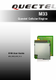
M33 Quectel Cellular Engine EVB User Guide M33_EVB_UGD_V1.
M33 EVB User Guide Document Title M33 EVB User Guide Version 1.0 Date 2010-06-28 Status Release Document Control ID M33_EVB_UGD_V1.0 l e t c l e a i t u Q den i f n o C General Notes Quectel offers this information as a service to its customers, to support application and engineering efforts that use the products designed by Quectel. The information provided is based upon requirements specifically provided to Quectel by the customers.
M33 EVB User Guide Contents 0. Revision History ...........................................................................................................................5 1. Introduction...................................................................................................................................6 1.1. Related Documents .............................................................................................................6 1.2. Safety Caution ....................................
M33 EVB User Guide Table Index TABLE 1: RELATED DOCUMENTS.....................................................................................................6 TABLE 2: PIN OF POWER INTERFACE ............................................................................................12 TABLE 3: PINS OF AUDIO CHANNEL 1 ...........................................................................................13 TABLE 4: PINS OF AUDIO CHANNEL 2 ................................................................
M33 EVB User Guide Figure Index FIGURE 1: EVB TOP VIEW (UNINSTALL M33-TE BOARD) ............................................................8 FIGURE 2: EVB TOP VIEW (INSTALLED M33_EVB_TE BOARD)..................................................8 FIGURE 3: EVB BOTTOM VIEW..........................................................................................................9 FIGURE 4: ACCESSORY INTRODUCTION.......................................................................................
M33 EVB User Guide 0. Revision History Revision Date Author Description of change 1.0 2010-06-28 Roy Chen Initial l e t c l e a i t u Q den i f n o C M33_EVB_UGD_V1.
M33 EVB User Guide 1. Introduction This document defines and specifies the usage of M33 EVB. 1.1. Related Documents Table 1: Related documents l e t c l e a i t u Q den i f n o C SN Document name Remark [1] M33_ATC AT commands set [2] GSM_UART_AN GSM UART port application notes [3] M33_HD M33 hardware design document [4] Upgrade_FW_Tools_UGD User guide of firmware upgrade tool [5] M33_Camera_ATC M33 AT Command set for camera function 1.2.
M33 EVB User Guide Cellular terminal or mobile receives and transmits radio frequency energy while switched on. RF interference could occur if it is close to TV set, radio, computer or other electronic equipments. Road safety comes first! Do not use a hand-held cellular terminal or mobile while driving a vehicle, unless it is securely mounted in a holder for hands-free operation. Park the vehicle before making a call with a hand-held terminal or mobile.
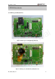
M33 EVB User Guide 2. EVB Kit Introduction 2.1. EVB Top and Bottom View l e t c l e a i t u Q den i f n o C Figure 1: EVB top view (Uninstall M33-TE board) Figure 2: EVB top view (Installed M33_EVB_TE board) M33_EVB_UGD_V1.
M33 EVB User Guide l e t c l e a i t u Q den i f n o C Figure 3: EVB bottom view A: B: C: D: E: F: G: H: I: J: K: L: M: N: O: P: Q: R: T: S: U: Serial Port 1 Serial Port 2 M33_EVB_TE Board interface (with indication mark) SIM card socket Test points Serial Port 3 Handset socket of audio channel 1 Headset socket of audio channel 2 Handset socket of PCM channel EMERG_OFF button Download switch ON/OFF button VCHG switch 5V power switch Power adapter interface Antenna connector fixing hole Screw holes for EV
M33 EVB User Guide 2.2. EVB Accessories l e t c l e a i t u Q den i f n o C Figure 4: Accessory introduction Figure 5: M33 EVB TE Board Accessory introduction A: B: C: D: 5V DC switching power supply USB to UART converter cable Antenna RF cable M33_EVB_UGD_V1.
M33 EVB User Guide E: F: G: H: Headset Screws for EVB placement M33 EVB TE Board Recommended camera module (OV7725 sensor, part number: CN003VEF2052 from Global Optics Limited) Note: Contact information of the camera module vendor is as follows: Global Optics Limited E-mail: shanghai@globaloptics.cn http://www.globaloptics.cn l e t c l e a i t u Q den i f n o C M33_EVB_UGD_V1.
M33 EVB User Guide 3. Interface Application 3.1. Power Interface l e t c l e a i t u Q den i f n o C Figure 6: Power interface Table 2: Pin of power interface Pin 1 Signal I/O Adapter input I Description 5V/2.5A DC source input 3.2. Audio Interface M33_EVB_UGD_V1.
M33 EVB User Guide Figure 7: Audio interface Table 3: Pins of audio channel 1 Pin Signal I/O Description 1 MIC1N I Negative microphone input 2 SPK1N O Negative receiver output 3 SPK1P O Positive receiver output 4 MIC1P I Positive microphone input l e t c l e a i t u Q den i f n o C Table 4: Pins of audio channel 2 Pin 1 2 3 4 Signal I/O AGND Description AGND of audio circuits AGND SPK2P O Positive receiver output MIC2P I Positive microphone input 3.3.
M33 EVB User Guide 2 RESERVE 3 SIM_IO I/O 4 SIM_CLK O SIM card clock 5 SIM_RST O SIM card reset 6 SIM_VDD O SIM card power output 8 SIM_PRESENCE I SIM card detection SIM card data I/O 3.4. Antenna Interface l e t c l e a i t u Q den i f n o C Figure 9: RF interface Figure 10: Antenna installation M33_EVB_UGD_V1.
M33 EVB User Guide 3.5. Serial Ports l e t c l e a i t u Q den i f n o C Figure 11: Serial Port 1& Serial Port 2 Figure 12: Serial Port 3 M33_EVB_UGD_V1.
M33 EVB User Guide Table 6: Pins of Serial Port 1 Pin Signal I/O 1_1 RS232_DCD1 O Data carrier detection 1_2 RS232_TXD1 O Transmit data 1_3 RS232_RXD1 I Receive data 1_4 RS232_DTR1 I Data terminal ready 1_5 GND 1_7 RS232_RTS1 I Request to send 1_8 RS232_CTS1 O Clear to send RS232_RI1 O Ring indicator 1_9 Description GND l e t c l e a i t u Q den i f n o C Note: The voltage level of the module’s Serial Ports signals has been shifted to RS-232 level, so it can be directly
M33 EVB User Guide 3.6. Switches and Buttons l e t c l e a i t u Q den i f n o C Figure 13: Switches and buttons Table 9: Switches and buttons Part S1 S2 S3 K1 K2 Name I/O 5V_ ON/OFF switch I VCHG I Control charge to a Li-ion or Li Polymer battery by the module. D/L I Place to ON when downloading firmware ON/OFF I Press this button for 2 seconds to turn on/off the module EMERG_OFF M33_EVB_UGD_V1.
M33 EVB User Guide 3.7. Operating Status LED l e t c l e a i t u Q den i f n o C Figure 14: Operating status indication LEDs Table 10: Operating status indication LEDs Part L1 L2 L3 Name I/O Description 5V ON/OFF indicator O On: VBAT ON Off: VBAT OFF Module Status indicator O On: module in power-on Off: module in power-off GSM_NET status indicator O Blinking differently to indicate various GSM network status M33_EVB_UGD_V1.
M33 EVB User Guide 3.8. Test Points l e t c l e a i t u Q den i f n o C Figure 15: Test points overview 3.8.
M33 EVB User Guide 3.8.2 J105 Test Points l e t c l e a i t u Q den i f n o C Figure 17: J105 test points Table 12: Pins of J105 Pin 1 2 3 4 5 6 7 8 9 10 3.8.3 Signal I/O Description EINT0 I External interrupt input 0 EINT1 I External interrupt input 1 STATUS O Indicate module status. High level indicates module power-on and low level indicates power-down.
M33 EVB User Guide Table 13: Pins of J102 Pin Signal I/O 1 KCOL0 I 2 KROW0 O 3 KCOL1 I 4 KROW1 O 5 KCOL2 I 6 KROW2 O 7 KCOL3 I KROW3 O KCOL4 I KROW4 O 8 9 10 3.8.
M33 EVB User Guide 3.8.5 J103 Test Points l e t c l e a i t u Q den i f n o C Figure 20: J103 test points Table 15: Pins of J103 Pin 1 2 3 4 5 6 7 8 9 10 Signal I/O Description RESERVE SPI_CS O Chip select of SD interface SPI_CLK O Serial clock of SD interface SPI_I I Data input of SD interface SPI_O O Data output of SD interface ADC0 I ADC input channel 0 RESERVE M33_EVB_UGD_V1.
M33 EVB User Guide 3.8.6 VDD_EXT and VBAT Test points l e t c l e a i t u Q den i f n o C Figure 21: VDD_EXT and VBAT test points Table 16: Pins of VBAT,VDD_EXT test points NET NAME VBAT VDD_EXT Description VBAT is the power supply of module Supply 2.8V voltage for external circuit. Note: Customer can test two test points to judge whether the power supply to the module or the VDD_EXT voltage from the module is correct or not. M33_EVB_UGD_V1.
M33 EVB User Guide 3.8.7 EVB_TE Board Interface l e t c l e a i t u Q den i f n o C Figure 22: EVB_TE Board Interface Table 17: Pins of TE Board interface X101 Pin 1 2 3 4 5 6 7 8 9 10 11 12 13 14 Signal I/O Description RESERVE SDA I/O I2C serial data RXD3 I Receives data of Serial Port 3 TXD3 O Transmit data of Serial Port 3 O Supply 2.8V voltage for external circuit.
M33 EVB User Guide Table 18: Pins of TE Board interface X102 Pin Signal 1 RESERVE 2 RESERVE 3 CS_SDA I/O I2C serial data of camera interface 4 CS_SCL O I2C serial clock of camera interface 5 CS_PIXCLK I Pixel clock input 6 CS_HSYNC I Horizontal synchronizing 7 CS_D6 8 9 10 11 12 13 14 15 16 17 18 19 20 I/O Description l e t c l e a i t u Q den i f n o C CS_D4 CS_D2 CS_D0 I YUV video data bus input CS_VSYNC I Vertical synchronizing CS_RESET O Reset camera module CS_PWDN
M33 EVB User Guide 4. EVB and Accessories The EVB and its accessories are shown as Figure 23. l e t c l e a i t u Q den i f n o C Figure 23: EVB and accessories (1) (2) (3) (4) (5) (6) (7) (8) Connect the RF cable to the RF connector of the module. Assembly the M33 module to the 100-pin connector on the M33 EVB. Fix the SMA connector of the RF cable in the connector fixing hole. Assembly SIM card to SIM card socket Assembly the M33_EVB_TE board on the M33 EVB.
M33 EVB User Guide l e t c l e a i t u Q den i f n o C Figure 24: EVB_TE Board accessories assembly A. B. X101 and X102 connectors of M33_EVB_TE board mark the direction of assembly. Install as instructed by Figure 24. The FPC cable of the camera module must be assembled in the way shown in Figure 24. M33_EVB_UGD_V1.
M33 EVB User Guide 5. Illustration 5.1. Power on Operations (1) Assembly the M33 module to the 100-pin connector on the M33 EVB. Put Switch S1 to ON state. Put Switch S2 to OFF position and Switch S3 to OFF position. Plug in 5V DC adapter. The LED L1 on the EVB will go bright. (2) Press the ON/OFF button for more than 2 seconds. When the STATUS_LED is lightened, and NET_LED is blinked , the module is working fine. l e t c l e a i t u Q den i f n o C 5.2.
M33 EVB User Guide Refer to Document [5] for more details of camera AT commands. 5.4. Firmware Upgrade (1) Start the Firmware Upgrade Tool in PC. (2) Press the START button in the Firmware Upgrade Tool. (3) Switch the S3 and S1 in the EVB to ON state as shown in Figure 25. After these steps, the firmware refreshing process will be proceeding. For more details, please refer to Document [4]. l e t c l e a i t u Q den i f n o C Figure 25: Switches state for firmware upgrade 5.5.
M33 EVB User Guide 6. 100 PIN Assignment of B2B Connector l e t c l e a i t u Q den i f n o C Figure 26: B2B connector of EVB Table 19: Pin definition of B2B connector PIN NO. PIN NAME I/O PIN NO.
M33 EVB User Guide 33 TXD3 O 34 MIC2N I 35 SPK1P O 36 MIC2P I 37 SPK1N O 38 MIC1N I 39 SPK2P O 40 MIC1P I 41 AGND 42 RESERVE 43 RESERVE 44 SCL O 45 STATUS 46 SDA I/O 47 RESERVE 48 GPIO3 I/O 49 EINT1 I 50 EINT0 I LIGHT_MOS O 52 RESERVE LED_B O 54 RESERVE 56 RESERVE 51 53 55 57 59 61 63 65 67 69 71 73 75 77 79 81 83 85 87 89 91 93 95 97 99 O l e t c l e a i t u Q den i f n o C RESERVE VIB O 58 LED_R O KCOL0 I 60 KCOL1 I KCOL2 I 62 KCOL
Quectel Wireless Solutions Co., Ltd. Room 501, Building 9, No. 99, Tianzhou Road, Shanghai, China 200233 Tel: +86 21 5108 2965 Mail: info@quectel.