
User guide


M33 EVB User Guide
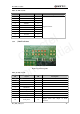
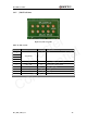
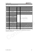
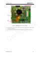
3.8.5 J103 Test Points
Figure 20: J103 test points
Table 15: Pins of J103
Pin Signal I/O Description
1
2
3
4
RESERVE
5 SPI_CS O Chip select of SD interface
6 SPI_CLK O Serial clock of SD interface
7 SPI_I I Data input of SD interface
8 SPI_O O Data output of SD interface
9 ADC0 I ADC input channel 0
10 RESERVE
M33_EVB_UGD_V1.0 - 22 -
Quectel
Confidential