MF1S50yyX MIFARE Classic 1K - Mainstream contactless smart card IC for fast and easy solution development Rev. 3.0 — 2 May 2011 196330 Product data sheet COMPANY PUBLIC 1. General description NXP Semiconductors has developed the MIFARE Classic MF1S50yyX to be used in a contactless smart card according to ISO/IEC 14443 Type A. The MIFARE Classic 1K MF1S50yyX IC is used in applications like public transport ticketing and can also be used for various other applications. 1.
MF1S50yyX NXP Semiconductors MIFARE Classic 1K - Mainstream contactless smart card IC 1.4 Delivery options • 7-byte UID, 4-byte NUID • bumped die on wafer • MOA4 and MOA8 contactless module 2. Features and benefits Contactless transmission of data and supply energy Operating frequency of 13.
MF1S50yyX NXP Semiconductors MIFARE Classic 1K - Mainstream contactless smart card IC 5. Ordering information Table 2.
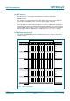
MF1S50yyX NXP Semiconductors MIFARE Classic 1K - Mainstream contactless smart card IC 7. Pinning information 7.1 Pinning The pinning for the MF1S50yyXDAx is shown as an example in Figure 3 for the MOA4 contactless module. For the contactless module MOA8, the pinning is analogous and not explicitly shown. LA top view LB 001aan002 Fig 3. Table 3.
MF1S50yyX NXP Semiconductors MIFARE Classic 1K - Mainstream contactless smart card IC 8. Functional description 8.1 Block description The MF1S50yyX chip consists of a 1 kB EEPROM, RF interface and Digital Control Unit. Energy and data are transferred via an antenna consisting of a coil with a small number of turns which is directly connected to the MF1S50yyX. No further external components are necessary. Refer to the document Ref. 1 for details on antenna design.
MF1S50yyX NXP Semiconductors MIFARE Classic 1K - Mainstream contactless smart card IC Remark: For the 4-byte non-unique ID product versions, the identifier retrieved from the card is not defined to be unique. For further information regarding handling of non-unique identifiers see Ref. 6. 8.2.3 Select card With the select card command the reader selects one individual card for authentication and memory related operations.
MF1S50yyX NXP Semiconductors MIFARE Classic 1K - Mainstream contactless smart card IC 8.2.
MF1S50yyX NXP Semiconductors MIFARE Classic 1K - Mainstream contactless smart card IC 8.5 RF interface The RF-interface is according to the standard for contactless smart cards ISO/IEC 14443A. For operation, the carrier field from the reader always needs to be present (with short pauses when transmitting), as it is used for the power supply of the card. For both directions of data communication there is only one start bit at the beginning of each frame.
MF1S50yyX NXP Semiconductors MIFARE Classic 1K - Mainstream contactless smart card IC 8.6.1 Manufacturer block This is the first data block (block 0) of the first sector (sector 0). It contains the IC manufacturer data. This block is programmed and write protected in the production test. The manufacturer block is shown in Figure 6 and Figure 7 for the 4-byte NUID and 7-byte UID version respectively. Block 0/Sector 0 Byte 0 1 2 3 4 5 6 7 NUID Fig 6.
MF1S50yyX NXP Semiconductors MIFARE Classic 1K - Mainstream contactless smart card IC • Adr: Signifies a 1-byte address, which can be used to save the storage address of a block, when implementing a powerful backup management. The address byte is stored four times, twice inverted and non-inverted. During increment, decrement, restore and transfer operations the address remains unchanged. It can only be altered via a write command.
MF1S50yyX NXP Semiconductors MIFARE Classic 1K - Mainstream contactless smart card IC 8.7 Memory access Before any memory operation can be done, the card has to be selected and authenticated as described in Section 8.2. The possible memory operations for an addressed block depend on the key used during authentication and the access conditions stored in the associated sector trailer. Table 5.
MF1S50yyX NXP Semiconductors MIFARE Classic 1K - Mainstream contactless smart card IC 8.7.1 Access conditions The access conditions for every data block and sector trailer are defined by 3 bits, which are stored non-inverted and inverted in the sector trailer of the specified sector. The access bits control the rights of memory access using the secret keys A and B. The access conditions may be altered, provided one knows the relevant key and the current access condition allows this operation.
MF1S50yyX NXP Semiconductors MIFARE Classic 1K - Mainstream contactless smart card IC 8.7.2 Access conditions for the sector trailer Depending on the access bits for the sector trailer (block 3) the read/write access to the keys and the access bits is specified as ‘never’, ‘key A’, ‘key B’ or key A|B’ (key A or key B). On chip delivery the access conditions for the sector trailers and key A are predefined as transport configuration.
MF1S50yyX NXP Semiconductors MIFARE Classic 1K - Mainstream contactless smart card IC 8.7.3 Access conditions for data blocks Depending on the access bits for data blocks (blocks 0...2) the read/write access is specified as ‘never’, ‘key A’, ‘key B’ or ‘key A|B’ (key A or key B). The setting of the relevant access bits defines the application and the corresponding applicable commands. • Read/write block: the operations read and write are allowed.
MF1S50yyX NXP Semiconductors MIFARE Classic 1K - Mainstream contactless smart card IC 9. Command overview The MIFARE Classic card activation follows the ISO/IEC 14443 Type A. After the MIFARE Classic card has been selected, it can either be deactivated using the ISO/IEC 14443 Halt command, or the MIFARE Classic commands can be performed. For more details about the card activation refer to Ref. 4. 9.
MF1S50yyX NXP Semiconductors MIFARE Classic 1K - Mainstream contactless smart card IC All timing can be measured according to ISO/IEC 14443-3 frame specification as shown for the Frame Delay Time in Figure 11. For more details refer to Ref. 3 and Ref. 4. The frame delay time from PICC to PCD must be at least 87 μs.
MF1S50yyX NXP Semiconductors MIFARE Classic 1K - Mainstream contactless smart card IC 9.4 ATQA and SAK responses For details on the type identification procedure please refer to Ref. 2. The MF1S50yyX answers to a REQA or WUPA command with the ATQA value shown in Table 11 and to a Select CL1 command (CL2 for the 7-byte UID variant) with the SAK value shown in Table 12. Table 11.
MF1S50yyX NXP Semiconductors MIFARE Classic 1K - Mainstream contactless smart card IC 10. UID Options and Handling The MF1S50yyX product family offers two delivery options for the UID which is stored in block 0 of sector 0. • 7-byte UID • 4-byte NUID (Non-Unique ID) This section describes the MIFARE Classic MF1S50yyX operation when using one of the 2 UID options with respect to card selection, authentication and personalization. See also Ref.
MF1S50yyX NXP Semiconductors MIFARE Classic 1K - Mainstream contactless smart card IC PCD Cmd Type CRC ACK PICC `ACK` 368 µs TACK 59 µs TNAK 59 µs NAK PICC `NAK` TTimeOut TimeOut 001aan919 Fig 12. Personalize UID Usage Table 13.
MF1S50yyX NXP Semiconductors MIFARE Classic 1K - Mainstream contactless smart card IC Table 15. Available activation sequences for 7-byte UID options UID Functionality Available Activation Sequences UIDF0 Sequence 1 UIDF1 Sequence 1, Sequence 2 UIDF2 Sequence 3 UIDF3 Sequence 3 10.1.3 Authentication During the authentication process, 4-byte of the UID are passed on to the MIFARE Classic Authenticate command of the contactless reader IC.
MF1S50yyX NXP Semiconductors MIFARE Classic 1K - Mainstream contactless smart card IC 11. MIFARE Classic commands 11.1 MIFARE Authentication The MIFARE authentication is a 3-pass mutual authentication which needs two pairs of command-response. These two parts, MIFARE authentication part 1 and part 2 are shown in Figure 13, Figure 14 and Table 17. Table 18 shows the required timing.
MF1S50yyX NXP Semiconductors MIFARE Classic 1K - Mainstream contactless smart card IC Table 18. MIFARE authentication timing These times exclude the end of communication of the PCD. TACK min TACK max TNAK min TNAK max TTimeOut 71 μs TTimeOut 1 ms Authentication part 1 71 μs TTimeOut Authentication part 2 71 μs TTimeOut 1 ms Remark: The minimum required time between MIFARE Authentication part 1 and part 2 is the minimum required FDT according to Ref. 4. There is no maximum time specified.
MF1S50yyX NXP Semiconductors MIFARE Classic 1K - Mainstream contactless smart card IC 11.3 MIFARE Write The MIFARE Write requires a block address, and writes 16 bytes of data into the addressed MIFARE Classic 1K block. It needs two pairs of command-response. These two parts, MIFARE Write part 1 and part 2 are shown in Figure 16 and Figure 17 and Table 21. Table 22 shows the required timing.
MF1S50yyX NXP Semiconductors MIFARE Classic 1K - Mainstream contactless smart card IC Table 22. MIFARE Write timing These times exclude the end of communication of the PCD. TACK min TACK max TNAK min TNAK max TTimeOut Write part 1 71 μs TTimeOut 71 μs TTimeOut 5 ms Write part 2 71 μs TTimeOut 71 μs TTimeOut 10 ms Remark: The minimum required time between MIFARE Write part 1 and part 2 is the minimum required FDT according to Ref. 4. There is no maximum time specified. 11.
MF1S50yyX NXP Semiconductors MIFARE Classic 1K - Mainstream contactless smart card IC PCD Data CRC PICC ,,ACK'' 538 μs NAK PICC ,,NAK'' 59 μs TNAK TTimeOut Time out 001aan009 (1) Increment, Decrement and Restore part 2 does not acknowledge Fig 19. MIFARE Increment, Decrement, Restore part 2 Table 23.
MF1S50yyX NXP Semiconductors MIFARE Classic 1K - Mainstream contactless smart card IC 11.5 MIFARE Transfer The MIFARE Transfer requires a destination block address, and writes the value stored in the volatile memory into one MIFARE Classic block. The command structure is shown in Figure 20 and Table 25. Table 26 shows the required timing. PCD Cmd Addr CRC ACK PICC ,,ACK'' 368 μs 59 μs TACK NAK PICC ,,NAK'' 59 μs TNAK TTimeOut Time out 001aan015 Fig 20. MIFARE Transfer Table 25.
MF1S50yyX NXP Semiconductors MIFARE Classic 1K - Mainstream contactless smart card IC 12. Limiting values Stresses above one or more of the limiting values may cause permanent damage to the device. Exposure to limiting values for extended periods may affect device reliability. Table 27. Limiting values In accordance with the Absolute Maximum Rating System (IEC 60134).
MF1S50yyX NXP Semiconductors MIFARE Classic 1K - Mainstream contactless smart card IC 14. Wafer specification For more details on the wafer delivery forms see Ref. 9. Table 29. Wafer specifications MF1S50yyXDUy Wafer diameter 200 mm typical (8 inches) maximum diameter after foil expansion 210 mm thickness MF1S50yyXDUD 120 μm ± 15 μm MF1S50yyXDUF 75 μm ± 10 μm flatness not applicable Potential Good Dies per Wafer (PGDW) est.
MF1S50yyX NXP Semiconductors MIFARE Classic 1K - Mainstream contactless smart card IC 14.2 Package outline For more details on the contactless modules MOA4 and MOA8 please refer to Ref. 7 and Ref. 8. PLLMC: plastic leadless module carrier package; 35 mm wide tape SOT500-2 X D A detail X 0 10 20 mm scale DIMENSIONS (mm are the original dimensions) UNIT A (1) max. D mm 0.33 35.05 34.95 For unspecified dimensions see PLLMC-drawing given in the subpackage code. Note 1.
MF1S50yyX NXP Semiconductors MIFARE Classic 1K - Mainstream contactless smart card IC PLLMC: plastic leadless module carrier package; 35 mm wide tape SOT500-4 X D A detail X 0 10 scale Dimensions Unit mm 20 mm A(1) D max 0.26 35.05 nom 35.00 min 34.95 For unspecified dimensions see PLLMC-drawing given in the subpackage code. Note 1. Total package thickness, exclusive punching burr.
MF1S50yyX NXP Semiconductors MIFARE Classic 1K - Mainstream contactless smart card IC 14.3 Bare die outline Chip Step x [mm] x [mm] 659(1) 694(1) 66 66 Bump size typ. 19,0(1) min.5,0 LA, LB, VSS, TEST typ. 19,0(1) min.5,0 240,8 MF1S50yyX LA 609,5 typ. 694,0(1) TESTIO 46,5 46,5 VSS LB 574,5 Y typ.659,0(1) X (1) the air gap and thus the step size may vary due to varying foil expansion (2) all dimensions in mm, pad locations measured from metal ring edge (see detail) 001aan924 Fig 23.
MF1S50yyX NXP Semiconductors MIFARE Classic 1K - Mainstream contactless smart card IC 15. Abbreviations Table 30.
MF1S50yyX NXP Semiconductors MIFARE Classic 1K - Mainstream contactless smart card IC 16. References 1.
MF1S50yyX NXP Semiconductors MIFARE Classic 1K - Mainstream contactless smart card IC 17. Revision history Table 31. Revision history Document ID Release date Data sheet status Change notice Supersedes MF1S50YYX v.3.0 20110502 Product data sheet - MF1S50YYX v.2.0 - - Modifications: MF1S50YYX v.2.0 MF1S50YYX Product data sheet COMPANY PUBLIC • General update 20101122 Preliminary data sheet All information provided in this document is subject to legal disclaimers. Rev. 3.
MF1S50yyX NXP Semiconductors MIFARE Classic 1K - Mainstream contactless smart card IC 18. Legal information 18.1 Data sheet status Document status[1][2] Product status[3] Definition Objective [short] data sheet Development This document contains data from the objective specification for product development. Preliminary [short] data sheet Qualification This document contains data from the preliminary specification.
MF1S50yyX NXP Semiconductors MIFARE Classic 1K - Mainstream contactless smart card IC Quick reference data — The Quick reference data is an extract of the product data given in the Limiting values and Characteristics sections of this document, and as such is not complete, exhaustive or legally binding. Non-automotive qualified products — Unless this data sheet expressly states that this specific NXP Semiconductors product is automotive qualified, the product is not suitable for automotive use.
MF1S50yyX NXP Semiconductors MIFARE Classic 1K - Mainstream contactless smart card IC 20. Tables Table 1. Table 2. Table 3. Table 4. Table 5. Table 6. Table 7. Table 8. Table 9. Table 10. Table 11. Table 12. Table 13. Table 14. Table 15. Table 16. Table 17. Table 18. Table 19. Table 20. Table 21. Table 22. Table 23. Table 24. Table 25. Table 26. Table 27. Table 28. Table 29. Table 30. Table 31. Quick reference data . . . . . . . . . . . . . . . . . . . . .2 Ordering information . . . . . . . . . . . . .
MF1S50yyX NXP Semiconductors MIFARE Classic 1K - Mainstream contactless smart card IC 21. Figures Fig 1. Fig 2. Fig 3. Fig 4. Fig 5. Fig 6. Fig 7. Fig 8. Fig 9. Fig 10. Fig 11. Fig 12. Fig 13. Fig 14. Fig 15. Fig 16. Fig 17. Fig 18. Fig 19. Fig 20. Fig 21. Fig 22. Fig 23. MIFARE card reader . . . . . . . . . . . . . . . . . . . . . . .1 Block diagram of MF1S50yyX . . . . . . . . . . . . . . . .3 Pin configuration for SOT500-2 (MOA4) . . . . . . . .4 Three pass authentication . . . . . . . . . . . . . .
MF1S50yyX NXP Semiconductors MIFARE Classic 1K - Mainstream contactless smart card IC 22. Contents 1 1.1 1.2 1.3 1.4 2 2.1 3 4 5 6 7 7.1 8 8.1 8.2 8.2.1 8.2.2 8.2.3 8.2.4 8.2.5 8.3 8.4 8.5 8.6 8.6.1 8.6.2 8.6.2.1 8.6.3 8.7 8.7.1 8.7.2 8.7.3 9 9.1 9.2 9.3 9.4 10 10.1 10.1.1 10.1.2 10.1.3 10.2 10.2.1 10.2.2 General description . . . . . . . . . . . . . . . . . . . . . . 1 Anticollision. . . . . . . . . . . . . . . . . . . . . . . . . . . . 1 Simple integration and user convenience. . . . . 1 Security. . .