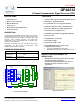
DATA SHEET QF4A512 4-Channel Programmable Signal Converter (PSC) APPLICATIONS • • • • • • FEATURES Wireless Sensor Networks • 4 Channel Analog 16-bit Programmable A/D Converter • Differential or Single Ended Inputs Machine Monitoring • 4 Programmable (1x, 2x, 4x, 8x) Gain Amplifiers Smart Sensors • Anti-Aliasing Filter Per Channel, 3rd Order Bessel Industrial Control Medical Monitoring and Diagnostics • Analog DC – 900kHz, up to 2Msps Sampling rate Homeland Security • Internal Precision Voltage
DATA SHEET QF4A512 TABLE OF CONTENTS 1. SPECIFICATIONS .............................................................................................................................................................. 4 1.1 ABSOLUTE MAXIMUM RATINGS ........................................................................................................................................ 4 1.2 PACKAGE ASSEMBLY .........................................................................................................
DATA SHEET QF4A512 9. SYSTEM CLOCKS ........................................................................................................................................................... 23 9.1 PLL CLOCK .................................................................................................................................................................. 24 9.2 SYSTEM CLOCK ......................................................................................................................
DATA SHEET QF4A512 1. SPECIFICATIONS 1.1 Absolute Maximum Ratings Stresses above those listed under Absolute Maximum Ratings can cause permanent device failure. Functionality at or above these limits is not implied. Exposure to absolute maximum ratings for extended periods may affect device reliability. Parameter Min Max Units Storage Temperature -60 125 ºC Supply Voltage, VDD18 to DGND -0.2V 2.2V V Supply Voltage, VDD33 with respect to DGND -0.2V 4.
DATA SHEET QF4A512 1.4 Electrical Characteristics Symbol Parameter (Condition) Min Typ Max Units Note Resolution N NMC Resolution, Nominal 16 Bits No Missing Codes Guaranteed 16 Bits DC Accuracy PSRR Power-supply rejection ratio 54 dB GERR Gain Error (Uncalibrated) 1 VOS DC Offset Error (Uncalibrated) - Chopper Off - Chopper On ±10 VREF Internal Voltage Reference 1.2 V 100 ppm/°C ± 0.
DATA SHEET Differential Input Capacitance QF4A512 10 Differential Input Resistance 4.6 5 pF 5.4 kΩ AV_PB Passband Attenuation (DC to 500 kHz) 0.2 dB GD Group Delay Variation (DC to 500 kHz) 5 % CI AN Channel Isolation, fADC = 50MHz fADC = 100MHz 75 35 Alias Noise Attenuation 4 dBc 45 dB 500 3 Anti-aliasing Filter Cutoff Frequency, aaf_freq=0 aaf_freq=1 kHz MHz Supply Current & Power Dissipation 1.8V Supply Operating Current IDD18 3.
DATA SHEET QF4A512 VOH High-level Output Voltage, DVDD18 = 1.6V, IOH = -100uA 1.4 V VOL Low-level Output Voltage, DVDD18 = 3.0V, IOL = 100uA 0.2 V CO Output Capacitance 10 pF CL Load Capacitance 20 pF 1. System calibration will reduce these errors to below the noise level. 2. System calibration at any temperature will eliminate this error. 3. Programmable Gain Amplifier set at a gain of x1, fIN = fs / 25 4. Input resistance may vary as much as +/-26% without calibration.
DATA SHEET QF4A512 1.6 Typical Performance Characteristics Default Conditions: TA = 25 C, VDD18 = 1.8V, VDD33 = 3.3V, unless otherwise noted. ENOB vs. Data Rate SINAD vs. Data Rate 14 90 13 12 SINAD (dB) ENOB (bits) 80 11 70 60 10 Chop OFF, 1.8V/3.3V Chop OFF, 1.8V/3.3V Chop ON, 1.8V/3.3V Chop ON, 1.8V/3.3V 9 50 1 10 Data Rate (kSPS) 100 1000 1 10 SFDR vs. Data Rate Data Rate (kSPS) 100 1000 SNR vs. Data Rate 90 100 90 80 SNR (dB) SFDR (dB) 80 70 70 60 60 Chop OFF, 1.
DATA SHEET QF4A512 Supply Current vs Number of Channels (3.3V) Supply Current vs Number of Channels (1.8V) 20 160 16 120 Supply Current (mA) Supply Current (mA) 80 12 8 40 4 1ksps 100ksps 2Msps 0 0 2 1 3 4 1 2 3 4 Number of Active Channels Number of Active Channels 2. PINOUT and PIN DESCRIPTIONS 2.
DATA SHEET 9 DVDD18 Power +1.8V DC Power (Digital) 10 DGND Ground Digital Ground 11 DGND Ground Digital Ground 12 /CS Input 13 DRDY/SEL Input/Output Chip Select from SPI Bus (Low logic selects chip). Internal pull-up. High when new data is ready, if pulled high accesses EEPROM direct. Internal pull-down. 14 SDO Output 15 SDI Input SPI Serial Data Input 16 SCLK Input SPI Clock (Maximum 40 MHz) 17 /RST Input Chip RESET (Low logic resets chip). Internal pull-up.
DATA SHEET QF4A512 3. GENERAL DESCRIPTION Figure 1. Functional Block Diagram 3.1 Analog Front End (AFE) The AFE consists of a Programmable Gain Amplifier (PGA), a chopper-stabilized amplifier and an Anti-Aliasing Filter. Programmable Gain Amplifier (PGA) The PGA can be set at gains of 1X, 2X, 4X, and 8X. The input impedance of the PGA is 10kΩ on both the positive and negative inputs. The PGA can be configured as either single ended or differential and can receive inputs of up to 2.0V p-p directly.
DATA SHEET QF4A512 The purpose of the CIH stage is droop recovery to compensate for the frequency response of the CIC filter. After moving through the CIH, the signals are sent into the FIR (Finite Impulse Response Filter) for user filtering. 3.3 Finite Impulse Response filter (FIR) The four FIR filters consist of 512 taps each and are individually programmable.
DATA SHEET QF4A512 Within EEPROM, 128 bytes of user space are provided for storing application-specific information. This data could include, for example, Transducer Electronic Data Sheets (TEDS, IEEE P1451.4). The full 14-bit address space can be accessed via the SPI interface in the "Configure" mode. In the "Run" mode only 8-bits of address space can be accessed, which include the command registers and other general configuration registers. 4. SOFTWARE 4.
DATA SHEET QF4A512 5. STARTUP The behavior of the QF4A512 during power up or after a reset can be determined by the configuration of 2 bits in the STARTUP_1 register. The auto_config bit, if set, will initiate transfer of EEPROM contents to the control registers and FIR filter coefficient RAMs. The auto_start bit will determine whether the chip starts in Run mode, filtering and sending data out on the SPI bus (auto_start=1), or the chip will wait in configure mode until manually started (auto_start=0).
DATA SHEET QF4A512 The sequence of events that occurs after a hardware reset is detailed in the preceding diagram. The hardware reset will be applied at power-up or when the external /RST pin is toggled low. If the DRDY pin is held high (for example to write directly to EEPROM) the startup sequence is bypassed. 5.2 Extended Initialization There is an option to perform an Extended Initialization regardless of the setting for auto_config.
DATA SHEET QF4A512 Note: The value in the IGC_SEQADDR registers can set in two ways. By default, if auto_config is not set it will take a value of F00h – corresponding to the start of User Memory. If auto_config is set it will be written to the value stored in the corresponding EEPROM address. The format for the sequences stored in EEPROM is shown in figure 4. The sequences must be in consecutive memory locations and consist of a series of addresses, each having a 16-bit (i.e 2 byte) value.
DATA SHEET QF4A512 6. ANALOG FRONT END (AFE) 6.1 Configurable parameters The following items are configurable for the AFE: 1. 2. 3. 4. Chopper on or off PGA Gain AAF Cutoff Frequency Channel on or off These settings can all be configured via the Quickfilter Pro software. 6.2 Chopper-stabilized Amplifier Low frequency flicker noise, which is inherent to CMOS devices, limits maximum dynamic range that can be attained solely by oversampling and averaging data from the analog front end (AFE).
DATA SHEET QF4A512 6.4 Input Voltage Levels Ideally the maximum input voltage to the QF4A512 should correspond to a full-scale reading from the ADC. If the input signal level is too low to achieve this, then PGA gain can be introduced to provide a larger signal to the ADC. If the input signal is too high then it should be attenuated to prevent clipping (see section 13 for suggested input circuit configurations).
DATA SHEET QF4A512 7. ANALOG TO DIGITAL CONVERTER 7.1 Overview The ADC has a pipeline architecture that is 12 bits in hardware and runs at up to 100Msps. Resolutions of up to 16 bits are achieved by oversampling the input and averaging the resultant conversions. With INL and DNL of +/- 1LSB, 16 bit linearity is achieved. During Chip Configuration and Filter Design, the exact sampling speed of the ADC is determined (based on the highest sampling rate required for any one of the four channels).
DATA SHEET QF4A512 The aggregate bandwidth is the total bandwidth available to all active channels. If only one channel is active then it can use the entire bandwidth, but as further channels are activated the bandwidth available to each will be reduced. Since the oversampling rate can be adjusted for each channel the bandwidth for that channel should be calculated based on its own effective sampling rate.
DATA SHEET QF4A512 7.9 User (System-level) Calibration Overall system level performance can be improved if a system level calibration is performed. Using this technique gain and offset errors introduced by variation in external components as well components internal to the QF4A512 itself can be minimized.
DATA SHEET QF4A512 8. FIR FILTERS 8.1 FIR Overview Each channel features a 512-tap FIR which is used to define the precise filtering characteristics desired. The filtering characteristics of each channel may be set independently may include any combination of the following types: lowpass, notched lowpass, highpass, bandpass, dual bandpass, bandstop, and dual bandstop. Currently available filter algorithms include Parks-McClellan and Windowed Sinc.
DATA SHEET QF4A512 8.3 FIR Latency There will be a delay introduced to the signal as it passes through the QF4A512. There are several components to this latency: 1. 2. 3. 4. 5. 6. PGA and AAF = If sample frequency FS is greater than 800kHz add 0.122uS, else add 0.
DATA SHEET QF4A512 which clocks are derived to drive the FIR filters, the ADC and the analog front end. The master clock is also divided down to provide a clock to be used for transfers to the on-chip EEPROM. PLL XTAL or EXT CLK OSC /1 f0 , 20MHz PLL_CTRL0 (1 – 64) Φ VCO 200MHz PLL_CLK /1 SYS_CLK 200MHz SYS_CLK_CTRL (1 – 64) /10 PLL_CTRL1 (1 – 64) /2 ADC_CLK 100MHz ADC_CLK_RATE (2 – 16) /16 EE_CLK 1.25MHz STARTUP_1 (1 – 32) Figure 7.
DATA SHEET QF4A512 The QF4A512 is designed to interface directly with the serial peripheral interface (SPI) of microcontrollers and Digital Signal Processors. The QF4A512 always operates in SPI slave mode where SDI is the input serial data, and SDO is the output serial data. SCLK is the input serial clock maximum 40 MHz. In order to address and write to the QF4A512, /CS is asserted low.
DATA SHEET QF4A512 Note, this data applies to SO and SI depending whether it is being read or written.
DATA SHEET QF4A512 10.3 Run Mode By setting the run_mode bit to 1 the QF4A512 is in Run mode, and will output converted and filtered data.. A 24-bit format is used including information and data (New Data Flag + Channel ID + 16 bits of data). The Serial Interface (SIF) will arbitrate between the incoming channels from the FIRs by monitoring each channels internal data ready signal.
DATA SHEET QF4A512 Table 13. Output Data, MSB, SD0 (00h-FFh) D23 D22 D21 D20 D19 D18 D17 D16 PARITY CH_ID CH_ID NEW adc_ov_L adc_ov adc_un_L adc_un Data23- Data16 = MSB of the 24 bit serial data. Description: This is the information byte showing which channel the data corresponds to, along with the new data flag and parity bit for valid data check.
DATA SHEET QF4A512 Figure 12. Run Mode Timing, Read and Write Note: Once set by the chip DRDY will remain high until /CS is pulled low. 10.4 Sending Commands in Run Mode Although Run mode exists primarily to output filtered data from the ADC it is also possible to issue commands to the QF4A512 in this mode.
DATA SHEET QF4A512 In Configure mode 14-bit address words are used. In Run mode 8-bit addressing is used. These differences are shown graphically in the following diagram. Consequently the host controller must use the appropriate timing depending on which mode of operation is active. (At power up the mode of operation is determined by the value of the auto_start bit (register STARTUP_1).
DATA SHEET QF4A512 11. EEPROM 11.1 Overview Table 14. EEPROM Memory Map User Data 0F80 (128 bytes) Chip Calibration 0F00 (128 Bytes) Filter Coefficient 0100 Data Control and 0007 status data 0000 Not used The internal EEPROM is used to store the QF4A512's FIR coefficients, general parameters and startup mode as well as have user space for application specific use, for example Transducer Electronic Data Sheets (TEDS).
DATA SHEET QF4A512 Multi-Byte Transfer Restrictions Reading from EEPROM A contiguous transfer will not proceed across the register map – coefficient memory boundary. In other words, you can’t cross 00FFh – 0100h within the block you are transferring. An easy solution is to break up the block into 2 block transfers, one up to 00FFh and the other starting with 0100h. Writing to EEPROM Starting with address 0000h, all block transfers must be on 32-byte boundaries (EEPROM limitation).
DATA SHEET QF4A512 Alternatively other user-specific information and/or formats can be stored in this area. The user data is not copied into chip RAM at power up. Since direct reads from EEPROM are not usually possible there are two methods to read/write the user data: a) Using the SCRATCH registers. The 8 registers starting at address 001Dh can be used to transfer data 8 bytes at a time, using the multi-byte transfer method described above. b) Using the data RAM at startup.
DATA SHEET QF4A512 Several registers are designated as “Reserved”. The user may write to these registers without any effect on chip operation, i.e. it is possible to write to the entire register map as a single contiguous block. However, when they are read these registers will return all ones or zeroes, not necessarily reflecting the value written to them during the write operation. The corresponding EEPROM locations can also be written, and these values can also be read back.
DATA SHEET QF4A512 02h FULL_SRST (Global Soft Reset) Bit 7 Bit 6 Bit 5 Bit 4 Bit 3 Bit 2 Bit 1 Address 02h X X X X X X X Bit 0 glbl_srst glbl_srst * 0 = Does nothing. 1 = Reset Description: Activates all soft resets. The reset value of this register is zero, regardless of the data in the corresponding EEPROM address.
DATA SHEET QF4A512 * 0 = default 1 = start transfer Description: Command to start transfer from EEPROM to registers/RAM. wr_strt * 0 = default 1 = start transfer Description: Command to start transfer from registers/RAM to EEPROM. rd_status * 0 = default 1 = start read of status register Description: Command to start read of EEPROM status register. Note: These command bits are automatically cleared by the chip after use.
DATA SHEET QF4A512 * 0 = Configure mode. 1 = Run mode Description: In Run mode automatically starts filtering and sending out filtered data on the SIF interface. Note: Bits 2 and 3 must be left at their default value of 0. eeclk_rate 000 (110, 111) = XTAL frequency 001 = XTAL frequency/2 010 = XTAL frequency/4 011 = XTAL frequency/8 *100 = XTAL frequency/16 101 = XTAL frequency/32 Description: Clock Rate for EEPROM data transfer. Frequency is divided down as shown above.
DATA SHEET QF4A512 pcg_chN_en *0 = Disabled 1 = Enabled Description: Enables the ADC clock and system clock for channel N. 0Ah ENABLE_1 (AAF Enable, ADC Mode) Bit 7 Bit 6 Address 0Ah X X Bit 5 Bit 4 Bit 3 Bit 2 Bit 1 Bit 0 afe_opmadc1 afe_opmadc0 afe_opmfec4 afe_opmfec3 afe_opmfec2 afe_opmfec1 afe_opmfecN * 0 = Powered Down 1 = Enabled Description: Enables the anti-aliasing filter for channel N. Must be enabled for the channel to be used, this bit is for power savings on disabled channels.
DATA SHEET QF4A512 Description: Indicates PLL lock status. ism_pll_lock – AUTO SET, may be reset by user * 0 = Not locked. 1 = Locked. Description: Indicates initialization lock status. 0Dh EE_VAL (EEPROM Status Register Value) – READ ONLY Bit 7 Bit 6 Bit 5 Bit 4 Bit 3 Bit 2 Bit 1 Bit 0 Address 0Dh D7 D6 D5 D4 D3 D2 D1 D0 Description: Value of the EEPROM Status register. Default value = 0 at powerup.
DATA SHEET QF4A512 adc_unN * 0 = No underflow. 1 = ADC underflow, out of range, low. Description: Indicates an underflow condition for the ADC on channel N. 12.5 Global Configuration Registers Table 17. Control Register listing (Global Configuration) Hex* Register Name 0011h PLL_CTRL_0 PLL Pre-divider, frequency range. Description 0012h PLL_CTRL_1 PLL loop divider. 0013h ADC_CLK_RATE Clock rate for ADC, CRC and AREC. 0014h SYS_CLK_CTRL System Clock control.
DATA SHEET QF4A512 adcclk_rate *00 = PLL clock/2 01 = PLLCLK/4 10 = PLLCLK/8 11 = PLLCLK/16 Description: Clock for the analog front end and ADC blocks. Afe_clk_inv *0 = No inversion 1 = Inverted Description: Inverts the clock input to the ADC. This setting should not be altered. 14h SYS_CLK_CTRL (System Clock Control) Bit 7 Bit 6 Bit 5 Address 14h X X X Bit 4 Bit 3 csifee_en X Bit 2 Bit 1 Bit 0 Sysclk_rate2 sysclk_rate1 sysclk_rate0 sysclk_rate *000 = PLL clock rate Description: System clock.
DATA SHEET QF4A512 1 = Enable Description: Enable address autoincrement. If set, on the next read/write cycle the address data can be followed by multiple data bytes. fast_ch *00 = Channel 1 01 = Channel 2 10 = Channel 3 11 = Channel 4 Description: Identifies the channel with the fastest sample rate. This channel is used to provide the DRDY signal. The user must ensure this channel is correctly identified and that the corresponding channel is enabled, otherwise missed data samples will result.
DATA SHEET Bit 7 Bit 6 Bit 5 Bit 4 Bit 3 Bit 2 Bit 1 QF4A512 Bit 0 Address 1Bh addr7 addr6 addr5 addr4 addr3 addr2 addr1 addr0 1Ch END_ADDR (Destination ending address - MSB) Bit 7 Bit 6 Address 1Ch X X Bit 5 Bit 4 Bit 3 Bit 2 Bit 1 Bit 0 addr13 addr12 addr11 addr10 addr9 addr8 Description: Destination ending address for block transfers. 12.6 Global Maintenance 1 Registers Table 18.
DATA SHEET Address 26h X X X QF4A512 pmux_srst arec_srst spim_rst iIgc_srst pcg_srst *0 = Default 1 = Reset Description: Soft reset of internal blocks. User resets can be performed in register FULL_SRST (02h).
DATA SHEET QF4A512 Run and Status Registers 30h CH1_PGA (Programmable Gain Amplifier Setting, FIR bypass) Bit 7 Bit 6 Bit 5 Address 30h X X X Bit 4 Bit 3 Bit 2 fir_0_1_bypass X X Bit 1 Bit 0 pga_gain1 pga_gain0 pga_gain * 00 = 1 01 = 2 10 = 4 11 = 8 Description: Sets the individual gain of the programmable gain amplifiers. The four settings are 1x 2x 4x or 8x the incoming signal. fir_0_1_bypass 0 = In-circuit *1 = Bypassed Description: Bypasses the main FIR filter (filter 1).
DATA SHEET QF4A512 *0 = No overflow 1 = Overflow Description: FIR, filter 1, input buffer overflow flag. fir_outsat0 *0 = Not saturated 1 = Saturated Description: FIR output saturation flag, filter 0. fir_outsat1 *0 = Not saturated 1 = Saturated Description: FIR output saturation flag, filter 1.
DATA SHEET QF4A512 Description: Enable FIR operation, filter 1. fir_0_0_bypass 0 = In-circuit *1 = Bypassed Description: Bypasses the FIR filter (filter 0). 33h AREC_1_GAIN (AREC gain control) Bit 7 Bit 6 Bit 5 Bit 4 Bit 3 Bit 2 Bit 1 Bit 0 Address 33h D7 D6 D5 D4 D3 D2 D1 D0 34h AREC_1_GAIN (AREC gain control) Bit 7 Bit 6 Bit 5 Bit 4 Bit 3 Bit 2 Bit 1 Bit 0 Address 34h D15 D14 D13 D12 D11 D10 D9 D8 Description: AREC gain control, default value = 4000.
DATA SHEET Address 3Ah X D6 D5 D4 D3 D2 D1 QF4A512 D0 Description: CIC shift value, default; value = 0. This is a function of the CIC “R” value and along with AREC_GAIN (33h, 34h) is calculated automatically by the Quickfilter Pro software. Note: The following registers (3Bh – 50h) have values generated by the Quickfilter Pro Design Software. Manual alteration of these registers is not recommended, the descriptions are for reference only.
DATA SHEET QF4A512 3Fh FIR_0_0_CMAX_F1 (Maximum coefficient storage address for f1) Bit 7 Bit 6 Bit 5 Address 3Fh X X Bit 4 Bit 3 Bit 2 Bit 1 Bit 0 addr5 addr4 addr3 addr2 addr1 addr0 Default value = 3F Description: Minimum and maximum coefficient storage address values for f1.
DATA SHEET QF4A512 fir_0_1_decimf1 Description: Decimation value for f1. Default value = 0, values in range 0 – 3. fir_0_1_decimf2 Description: Decimation value for f2. Default value = 0, values in range 0 – 3.
DATA SHEET QF4A512 4Dh FIR_0_1_NMAX_F2 (Maximum storage address for f2) Bit 7 Bit 6 Bit 5 Bit 4 Bit 3 Bit 2 Bit 1 Bit 0 Address 4Dh addr7 addr6 addr5 addr4 addr3 addr2 addr1 addr0 4Eh FIR_0_1_ NMAX_F2 (Maximum storage address for f2) Bit 7 Bit 6 Bit 5 Bit 4 Bit 3 Bit 2 Bit 1 Bit 0 Address 4Eh X X X X X X X addr8 Default value =1FF Description: Maximum data storage (tap) address value for f2.
DATA SHEET QF4A512 Description: Soft reset the FIR block, filter 0. fir_0_1_srst *0 = No action 1 = Reset Description: Soft reset the FIR block, filter 1.
DATA SHEET QF4A512 Default value = 8000 Description: Gain calibration value is written here. 5Ah – 5Fh – Reserved The following registers implement similar functionality for the three remaining channels. Please refer to the descriptions above. 60h – 8Fh Channel 2 Registers (see 30h – 5Fh for functionality) 90h – BFh Channel 3 Registers (see 30h – 5Fh for functionality) C0h – E9h Channel 4 Registers (see 30h – 5Fh for functionality) 12.8 Global Maintenance 2 Registers Table 21.
DATA SHEET QF4A512 1 = Gain calibration Description: Select whether to perform gain or offset calibration. cal_enab *0 1 = Start Description: Write to 1 to begin calibration. cal_srst *0 1 = Reset Description: Soft reset the calibration block.
DATA SHEET QF4A512 100h FIR_0_0_COEF_RAM (Coefficients for G Filter Channel 1, LSB) Bit 7 Bit 6 Bit 5 Bit 4 Bit 3 Bit 2 Bit 1 Bit 0 Channel1 100h C1TG1_7 C1TG1_6 C1TG1_5 C1TG1_4 C1TG1_3 C1TG1_2 C1TG1_1 C1TG1_0 Channel2 180h C2TG1_7 C2TG1_6 C2TG1_5 C2TG1_4 C2TG1_3 C2TG1_2 C2TG1_1 C2TG1_0 Channel3 200h C3TG1_7 C3TG1_6 C3TG1_5 C3TG1_4 C3TG1_3 C3TG1_2 C3TG1_1 C3TG1_0 Channel4 280h C4TG1_7 C4TG1_6 C4TG1_5 C4TG1_4 C4TG1_3 C4TG1_2 C4TG1_1 C4TG1_0 *Note, Failure to writ
DATA SHEET QF4A512 (C1TH1_0 - C1TH1_7): Represents the LSB in half of TAP1 Coefficient Data for Channel 1. Description: This is the LSB of the 16 bit Coefficient Data for the first unique TAP value. The H filter has a fixed set of 89 taps. Because the Taps are mirrored, only 45 unique 16 bit coefficients are stored. Since this is an odd number of taps, you have to add 1 to 89= 90/2 = 45. The starting address for the H filter is after the G filter coefficients end.
DATA SHEET QF4A512 301h FIR_0_1_COEF_RAM (Coefficients for FIR Filter per Channel, Byte 2) Bit 7 Bit 6 Bit 5 Bit 4 Bit 3 Bit 2 Bit 1 Bit 0 Channel1 301h C1T1_15 C1T1_14 C1T1_13 C1T1_12 C1T1_11 C1T1_10 C1T1_9 C1T1_8 Channel2 601h C2T1_15 C2T1_14 C2T1_13 C2T1_12 C2T1_11 C2T1_10 C2T1_9 C2T1_8 Channel3 901h C3T1_15 C3T1_14 C3T1_13 C3T1_12 C3T1_11 C3T1_10 C3T1_9 C3T1_8 Channel4 C01h C4T1_15 C4T1_14 C4T1_13 C4T1_12 C4T1_11 C4T1_10 C4T1_9 C4T1_8 *Note, Failure to write
DATA SHEET QF4A512 1400h FIR_0_1_DATA_RAM (FIR Data Memory, LSB) Bit 7 Bit 6 Bit 5 Bit 4 Bit 3 Bit 2 Bit 1 Bit 0 Channel1 1400h C1D1_7 C1D1_6 C1D1_5 C1D1_4 C1D1_3 C1D1_2 C1D1_1 C1D1_0 Channel2 1800h C2D1_7 C2D1_6 C2D1_5 C2D1_4 C2D1_3 C2D1_2 C2D1_1 C2D1_0 Channel3 1C00h C3D1_7 C3D1_6 C3D1_5 C3D1_4 C3D1_3 C3D1_2 C3D1_1 C3D1_0 Channel4 2000h C4D1_7 C4D1_6 C4D1_5 C4D1_4 C4D1_3 C4D1_2 C4D1_1 C4D1_0 (C1D1_0 - C1D1_7): Represents the LSB of a 16 bit value of in this ca
DATA SHEET QF4A512 12.10 Register Listing 00H GLBL_SW (USER REGISTER) .......................................................................................................................................... 34 01H GLBL_ID (CHIP ID) - READ ONLY................................................................................................................................. 34 02H FULL_SRST (GLOBAL SOFT RESET) ..................................................................................................
DATA SHEET QF4A512 41H FIR_0_0_NMAX_F2 (MAXIMUM STORAGE ADDRESS FOR F2)............................................................................................ 49 42H FIR_0_0_CMIN_F2 (MINIMUM COEFFICIENT STORAGE ADDRESS FOR F2) .......................................................................... 49 43H FIR_0_0_CMAX_F2 (MAXIMUM COEFFICIENT STORAGE ADDRESS FOR F2) ....................................................................... 49 44H FIR_0_1_CTRL (FIR CONTROL, FILTER 1) ...................
DATA SHEET QF4A512 13. APPLICATION CIRCUITS For more information please see Application note QFAN004 at http://www.quickfiltertech.com/html/app_notes.php 13.1 AC Coupled, Single-ended Input (0 - 2V AC) C1 R1 PGA x1 AC Coupled 0 3.3uF J1 BNC C2 1 CH 1 1V8 0 0.1 uF C10 3V3 C11 0.1 uF 0603 0603 3.3uF 2 Single Ended 1V8 R2 C9 1 CH 3 R6 1V8 25 A4N DGND QF4A512 RSTN C13 23 18 pF 0603 TP1 18 pF 22 1V8 0603 21 20 3V3 C14 0.1uF 0603 19 18 1V8 C15 0.
DATA SHEET QF4A512 13.2 DC coupled, Single-ended Input (0 - 3.3V DC) PGA x1 DC swing needs to be between (0.5 to 2.5) V R5 Internal impedance 10K connected to 1.2V Single Ended J1 BNC CH 1 DC Coupled 23.2K 1% 1 1V8 R1 23.2K 1% 1V8 0.1 uF C10 3V3 C11 0.1 uF 0603 2 0603 C9 0.1uF 0603 CH 3 1 R3 1V8 25 PGND A4N QF4A512 DGND 18 pF 0603 TP1 C13 23 18 pF 22 1V8 0603 21 20 3V3 C14 0.1uF 0603 19 18 1V8 C15 0.
DATA SHEET QF4A512 13.3 AC coupled, Differential Input (10V AC) PGA x2 C1 R1 AC Coupled 90K 1% 3.3uF 2 C2 1 CH 1 1V8 R2 3V3 90K 1% J1 3.3uF Differential 1V8 0.1 uF C10 C11 0.1 uF 0603 0603 BNC C9 1V8 25 A4N QF4A512 DGND C13 23 18 pF 0603 TP1 18 pF 22 1V8 0603 21 20 3V3 C14 0.1uF 0603 19 18 1V8 C15 0.1uF 0603 17 SCLK RSTN SDI A4P C12 1 1 PGND 27 28 26 PVDD18 AGND AVDD18 29 AVDD18 30 AGND 31 DVDD18 X1 20.000 MHz HCM49-20.000MABJT 24 C16 0.
DATA SHEET QF4A512 13.4 DC coupled, Differential Input (+/-1V DC) R1 PGA x2 Input (-1V to +1V DC) 10K 1% DC Coupled PGA x2 2 1V8 1 CH 1 0.1 uF C10 C11 0.1 uF 0603 3V3 10K 1% J1 Differential 1V8 R2 0603 BNC C9 0.1uF 0603 25 DGND QF4A512 18 pF 0603 TP1 C13 23 18 pF 22 1V8 0603 21 20 3V3 C14 0.1uF 0603 19 18 1V8 C15 0.1uF 0603 17 SCLK SDI RSTN SDO A4P DRDY/SEL A4N C12 1 1 PGND 26 PVDD18 27 AGND 28 AVDD18 29 AVDD18 30 AGND 31 AGND DVDD18 A3P X1 20.
DATA SHEET QF4A512 14. PACKAGING INFORMATION 7x7x1.4mm, LQFP 32, 0.8 mm Pitch POD (JEDEC) Dimension Minimum (mm) Maximum (mm) A 1.4 1.6 A1 0.05 0.15 A2 1.35 1.45 b 0.3 0.45 b1 0.3 0.4 c 0.09 0.2 c1 0.09 0.178 Notes: 1. Dimensions are in millimeters. 2. Interpret dimensions and tolerance per ASME Y14.5M1994 3. Datum Plane H is located at bottom of lead and is coincident with the lead where the lead exits the plastic body at the bottom of the parting line. D 9 BSC 4.
DATA SHEET QF4A512 List of Figures FIGURE 1. FUNCTIONAL BLOCK DIAGRAM.................................................................................................................................. 11 FIGURE 2. MEMORY MAP ......................................................................................................................................................... 12 FIGURE 3. POWER UP / RESET SEQUENCE .............................................................................................
DATA SHEET QF4A512 The contents of this document are provided in connection with Quickfilter Technologies, Inc. products. Quickfilter makes no representations or warranties with respect to the accuracy or completeness of the contents of this publication and reserves the right to make changes to specifications and product descriptions at any time without notice. No license, whether express, implied, arising by estoppel or otherwise, to any intellectual property rights is granted by this publication.