
User`s manual

User’s Manual 51
4.4 Jackrabbit Function Calls
4.4.1 I/O Drivers
The Jackrabbit contains four high-power digital output channels, two D/A converter out-
put channels, and one A/D converter input channel. These I/O channels can be accessed
using the functions found in the JRIO.LIB library.
4.4.1.1 Initialization
The function jrioInit() must be called before any other function from the JRIO.LIB
library. This function initializes the digital outputs and sets up the driver for the analog
input/outputs. The digital outputs correspond to the Rabbit processor’s port E bits 0–3, and
the analog I/O uses timer B; bits 1, 2, and 4 of port D; and bits 6 and 7 of port E.
The function void jrioInit() initializes the I/O drivers for Jackrabbit. In particular, it
sets up parallel port D bits 1, 2, and 4 for analog output, port E bits 0–3 for digital output,
and starts up the pulse-width modulation routines for the A/D and D/A channels. Note that
these routines can consume up to 20% of the CPU’s processing power; the routines use
timer B and the B1 and B2 match registers.
4.4.1.2 Digital Outputs
The Jackrabbit contains four high-power digital output drivers, HV0–HV3, on header J4.
These can be turned on and off with the following functions from the library JRIO.LIB.
HV0, HV1, and HV2 are open-collector sinking outputs, and are able to sink up to 1 A
(200 mA for the Jackrabbit and BL1820)
from a 30 V source connected to the K line on
header J4. HV3 is a sourcing output that is able to source up to 500 mA (100 mA for the
BL1810 and BL1820) from a 30 V source connected to the K line.
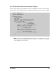
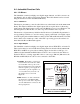
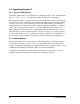
CAUTION: Remember to cut the trace
between K and Vcc inside the outline
for header JP2 on the top side of the
Prototyping Board if you are supplying
K from a separate power supply. An
exacto knife, a precision grinder tool,
or a screwdriver may be used to cut
through the traces as shown in
Figure 16.
NOTE: Failure to do this could lead to
the destruction of the Rabbit 2000
microprocessor and other components
once the Jackrabbit is connected to the
Prototyping Board.
Figure 16. Cut Trace on Prototyping Board
When Vcc and K Are Different
Cut gray trace
as shown
Cut
Buzzer
Top Side
Prototyping
Board
JP2
1
2
3
R3
R1
LS1
RT1
BZR
VCC
K
AD0
PE4
POT
HV0
+RAW
COIL(-)
PD0
GND
AD0
+
JP2
K
VCC