
User`s manual


User’s Manual 145
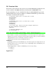
B.3 Chip Select Circuit
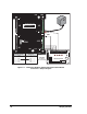
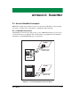
Figure B-5 shows a schematic of the chip select circuit on the OP7200’s RabbitCore module.
Figure B-5. Chip Select Circuit
The current drain on the battery in a battery-backed circuit must be kept at a minimum.
When the OP7200 is not powered, the battery keeps the SRAM memory contents and the
real-time clock (RTC) going. The SRAM has a powerdown mode that greatly reduces
power consumption. This powerdown mode is activated by raising the chip select (CS)
signal line. Normally the SRAM requires Vcc to operate. However, only 2 V is required
for data retention in powerdown mode. Thus, when power is removed from the circuit, the
battery voltage needs to be provided to both the SRAM power pin and to the CS signal
line. The CS control circuit accomplishes this task for the SRAM’s chip select signal line.
In a powered-up condition, the CS control circuit must allow the processor’s chip select
signal /CS1 to control the SRAM’s CS signal /CSRAM. So, with power applied, /CSRAM
must be the same signal as /CS1, and with power removed, /CSRAM must be held high
(but only needs to be battery voltage high). Q3 and Q4 are MOSFET transistors with com-
plementary polarity. They are both turned on when power is applied to the circuit. They
allow the CS signal to pass from the processor to the SRAM so that the processor can peri-
odically access the SRAM. When power is removed from the circuit, the transistors will
turn off and isolate /CSRAM from the processor. The isolated /CSRAM line has a 100 kΩ
pullup resistor to VRAM (R28). This pullup resistor keeps /CSRAM at the VRAM voltage
level (which under no power condition is the backup battery’s regulated voltage at a little
more than 2 V).
Transistors Q3 and Q4 are of opposite polarity so that a rail-to-rail voltage can be passed.
When the /CS1 voltage is low, Q3 will conduct. When the /CS1 voltage is high, Q4 con-
ducts. It takes time for the transistors to turn on, creating a propagation delay. This propa-
gation delay is typically very small, about 10 ns to 15 ns.
/CS1
/CSRAM
/RES
_
OUT
Q3
Q4
R28
VRAM
100 kW
VRAM
SWITCH