
User's Manual
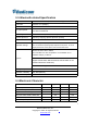
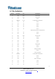
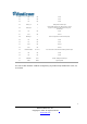

3.7 Pin Definition
Pin No. Pin Name I/O Description
01 GND Power System ground
02 GND Power System ground
03 P32
I/O Port 32
04 P38/MOSI I/O / O Port 38 / MOSI for SPI Interface
05 P12 I/O Port 12
06 P10 I/O Port 10
07 P17 I/O Port 17
08 P16 I/O Port 16
09 P11 I/O Port 11
10 NC Module internal connection for write protection
11 P26 I/O Port 26
12 P27 I/O Port 27
13 3P0V Power 3V power output
14 P33 I/O Port 33
15 P28 I/O Port 28
16 P29 I/O Port 29
17 P15 I/O Port 15
18 GND Power System ground
19 P14 I/O Port 14
20 P18 I/O Port 18
21 VBAT Power Battery power supply
22 P20 I/O Port 20
23 SCL O
SCL for I²C Interface
24 P25/MISO I/O / I Port 25 / MISO for SPI Interface
25 P19 I/O Port 19
26 P13 I/O Port 13
27 SDA I/O
SDA for I²C Interface
28 P0 I/O Port 0
29 P24 I/O Port 24
30 P5 I/O Port 5
8
Radicom Research, Inc.
Copyright © 2014. All rights
reserved
www.radi.com