
Data Sheet


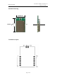


Table Of Contents

RC-S2
LP-915 Module Datasheet V1.1
February 27, 2019
Pa
d
N
umber
N
ame
D
escription
P
in Type
1
SD
O
SP
I slave data output
D
igital out
2
SD
I
SP
I slave data input
D
igital in
3
SC
LK
SP
I slave clock input
D
igital in
4
C
Sn
SP
I chip select
D
igital in
5
GPIO0
G
eneral purpose I/O that may be
configured through the SPI
registers to perform various functions
D
igital I/O
6
GPIO1
G
eneral purpose I/O that may be
configured through the SPI
registers to perform various functions
D
igital I/O
7
GPIO2
G
eneral purpose I/O that may be
configured through the SPI
registers to perform various functions
D
igital I/O
8
GPIO3
G
eneral purpose I/O that may be
configured through the SPI
registers to perform various functions
D
igital I/O
9
G
ND
C
onnect to GND
G
round pin
10
SD
N
S
hutdown input pin. SDN should be = ‘0’ in all
modes, but SHUTDOWN mode
D
igital in
11
G
ND
C
onnect to GND
G
round pin
12 GND Connect to GND Ground pin
13
VC
C
1
.8 V to 3.6 V power
P
ower Supply
14 VCC 1.8 V to 3.6 V power Power Supply
15
G
ND
C
onnect to GND
G
round pin
16
G
ND
C
onnect to GND
G
round pin
17
G
ND
C
onnect to GND
G
round pin
18
G
ND
C
onnect to GND
G
round pin
19
G
ND
C
onnect to GND
G
round pin
20
A
NT
C
onnect to an external Antenna
A
ntenna
Interface
21
G
ND
C
onnect to GND
G
round pin
Page 5 of 11
Radiocontrolli SRL